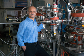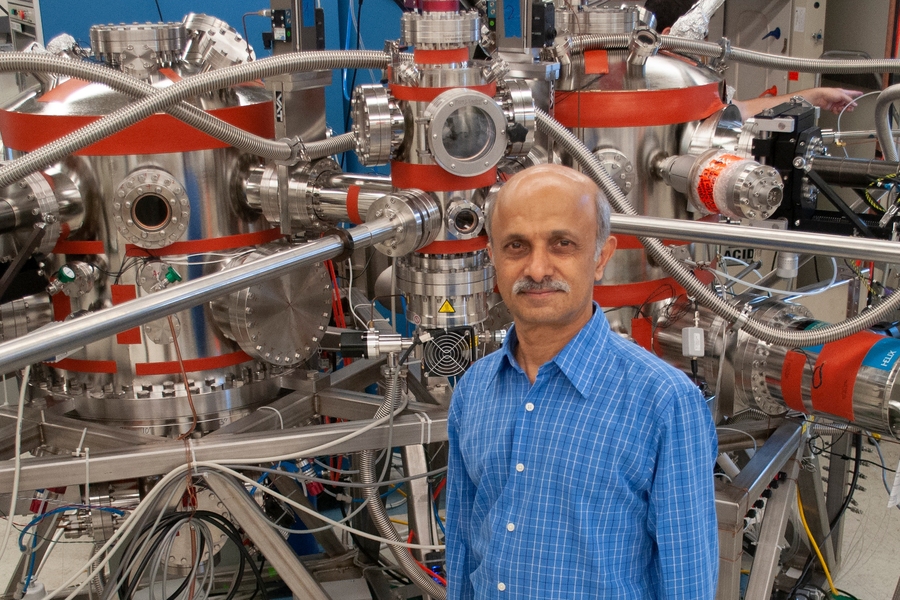
When ultrathin layered materials are coupled with other quantum materials having different properties, the resulting interface could produce a new quantum phenomenon — and new properties of the hybrid system could be unprecedented. This rich interface phenomenon is the topic of new investigation by Jagadeesh Moodera and his group at MIT's Plasma Science and Fusion Center.
“Surface and interface play pivotal roles in many of the recently discovered quantum phenomena in condensed matter physics,” Moodera points out. “Investigating the complex interface behavior when two quantum systems are coupled is a treasure island to be explored for new discoveries and for advancing the field.”
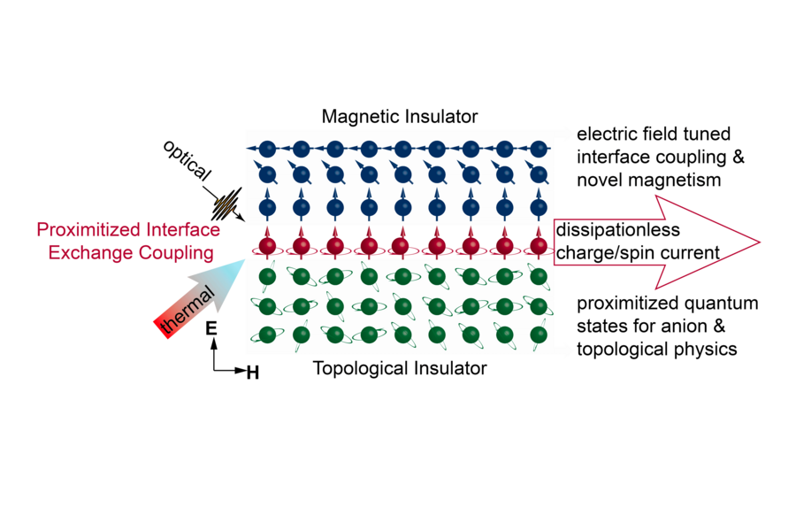
Moodera’s group has extensive experience studying quantum interfaces, having discovered in 2016 that coupling ultrathin layers of topological insulators (TI) — where electrons flow freely but only on the surface — with ferromagnetic or superconducting layers dramatically affects the behavior of each layer. Most recently they've explored the surface superconductivity in nanostructures of gold in proximity to the superconductor vanadium and a ferromagnetic insulator, in the quest to create the enigmatic Majorana fermion pair.
New multiyear funding and an equipment grant from the U.S. Department of Defense (DoD) Army Research Office will support novel work exploring the behavior that arises at the interface of quantum materials, and will help uncover ways to tune these new properties to develop future quantum electronics. Working closely with Argonne, Brookhaven, and Oak Ridge national laboratories advanced facilities, Moodera's group will explore interface effects, such as “interfacial exchange coupling,” with the goal of creating energy-efficient quantum devices.
As part of the DoD project, they will work with scientists at the Army Research Lab (ARL) in Maryland to build an ultraclean, atomically groomed multifunctional hybrid materials platform to probe the interplay between various quantum phenomena. They will experiment with tuning the interface to create quantum materials for building devices that could, for example, operate faster and use less energy. Moodera anticipates that some results may lead them into unexpected territory, possibly guiding them to even more surprising observations in quantum materials.
“If we can build new devices with two-dimensional quantum materials that have desirable properties, such as graphene or TI, and change their state for memory and logic with electric fields rather than actual flowing current, we will have gained a big advantage over conventional electronics.”
This could lead to greatly improved quantum electronics, including quantum sensors, memories, and interconnects. It could benefit computer microprocessors, which contain hundreds of millions of transistors that are affected by heat generated in them by conventional electronics, and powerful computer data storage banks, which consume about 2-3 percent of all the electrical power in the country.
Moodera looks forward to working with postdocs Hang Chi (visiting from ARL) and Yunbo Ou, along with instrument scientist Valeria Lauter from Oak Ridge National Laboratory, visiting scientist from Northeastern University Don Heiman, and other worldwide collaborators. He is excited about the possibilities their new research will uncover.
“Our DoD-supported project allows us to explore exciting physics and to address important scientific questions at the atomic scale, advancing experimental knowledge and theoretical understanding,” he says. “We aim to build a safer, sustainable, and energy-efficient future quantum information system, one layer at a time.”