
In 1951, the Department of Defense (DoD) needed a homeland air defense system. To develop one, they partnered with MIT to create Lincoln Laboratory, the federally-funded research and development center, where the nation’s first air defense system, SAGE, was successfully prototyped.
In the nearly 70 years since then, the laboratory has continued to innovate technology for the nation — radars, imagers, lasers, and microelectronics that are key to modern defense systems. As technology has progressed, however, some Lincoln Laboratory facilities have not: The original 1950s buildings still make up nearly half the square footage of the laboratory.
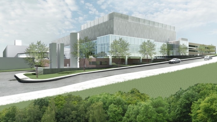
In 2014, the DoD acknowledged a critical need for facility modernizations following seven years of independent third-party and government studies. As a result, Lincoln Laboratory and the DoD developed a phased facility modernization plan that will allow the laboratory to continue to field state-of-the-art capabilities to address national security needs. The first building will replace critical, yet aging, labs with a new Compound Semiconductor Laboratory and Microsystem Integration Facility (CSL-MIF). The second building will replace aging and distributed prototyping spaces with a modern Engineering Prototyping Facility (EPF).
In 2017, $40 million of military construction funding was appropriated for the planning and design of the two buildings. Construction of the CSL-MIF will be completed with $90 million of funding from the fiscal year 2019 Consolidated Appropriations Act and an additional $135 million of funding from the fiscal year 2020 President’s Budget Request. The EPF construction funds are programmed in fiscal year 2022.
“This funding will allow Lincoln Laboratory to modernize and improve their facilities, giving some of the best minds and talent confronting our nation’s most complex technological challenges a modern, state-of-the-art laboratory in which to work,” former Massachusetts Congresswoman Niki Tsongas stated in a press release in 2016 when initial funding was announced.
Craig Keast, the associate head of the Advanced Technology Division, which will oversee the CSL-MIF facility, says that the project “will provide a state-of-the-art advanced electronics research and prototyping facility targeted at developing and demonstrating complex electronic prototypes suitable for integration into ground, airborne, and spaceborne demonstration systems of interest to the DoD.”
The design plans include approximately 150,000 square feet of new cleanroom space, where scientists and engineers can grow non-silicon-based semiconductor material, package optics, assemble focal plane arrays, and mount complex semiconductor devices. These electronic and photonic devices will be joined with micromechanical components in the microsystem integration facility, resulting in prototypes of complete systems. Technologies of focus will include focal plane arrays for wide-area surveillance, qubit integration technology for quantum computers, and 3-D imaging systems, among several other key projects.
The CSL-MIF will complement Lincoln Laboratory’s existing silicon-based Microelectronics Laboratory (ML), which is regarded as the government’s best microelectronics facility.
“The combination of the CSL-MIF and ML facilities along with the laboratory’s excellent research staff, and their deep understanding of the broader DoD mission space, will provide the DoD with its premier advanced electronics research and prototyping capability,” Keast adds “and help ensure the DoD’s continued superiority in this core technology area.”
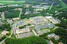
The CSL-MIF construction contract is scheduled to be awarded in September by the Army Corps of Engineers. It will be built on Hanscom Air Force Base, where Lincoln Laboratory’s 1.75 million-square-foot main campus is housed.
The second building of the facility modernization plan, the EPF, will be constructed beginning in 2022. This facility will consolidate distributed engineering spaces and clean rooms and enhance the high-bay prototyping capabilities of the laboratory. A third phase of the plan is in the early stages of concept development and will modernize the remaining aging parts of the laboratory over the next 30 years.
“Modern purpose-built facilities are critical for leading-edge research,” says Scott Anderson, the assistant director for operations at Lincoln Laboratory. “The CSL-MIF and the EPF projects are critical steps in rehabilitating the MIT Lincoln Laboratory complex. MIT Lincoln Laboratory has effectively advanced technology for national security in key mission areas for nearly 70 years, and these facilities will allow that to continue for next 50.”