Researchers have tried a variety of methods to develop detectors that are responsive to a broad range of infrared light — which could form imaging arrays for security systems, or solar cells that harness a broader range of sunlight’s energy — but these methods have all faced limitations. Now, a new system developed by researchers at five institutions, including MIT, could eliminate many of those limitations.
The new approach is described in a paper published in the journal Nature Communications by MIT graduate student Jonathan Mailoa, associate professor of mechanical engineering Tonio Buonassisi, and 11 others.
Silicon, which forms the basis of most semiconductor and solar-cell technology, normally lets most infrared light pass right through. This is because the material’s bandgap — a fundamental electronic property — requires an energy level greater than that carried by photons of infrared light. “Silicon usually has very little interaction with infrared light,” Buonassisi says.
Various treatments of silicon can mitigate this behavior, usually by creating a waveguide with structural defects or doping it with certain other elements. The problem is that most such methods have significant negative effects on silicon’s electrical performance; only work at very low temperatures; or only make silicon responsive to a very narrow band of infrared wavelengths.
The new system works at room temperature and provides a broad infrared response, Buonassisi says. It incorporates atoms of gold into the surface of silicon’s crystal structure in a way that maintains the material’s original structure. Additionally, it has the advantage of using silicon, a common semiconductor that is relatively low-cost, easy to process, and abundant.
The approach works by implanting gold into the top hundred nanometers of silicon and then using a laser to melt the surface for a few nanoseconds. The silicon atoms recrystallize into a near-perfect lattice, and the gold atoms don’t have time to escape before getting trapped in the lattice.
In fact, the material contains about 1 percent gold, an amount more than 100 times greater than silicon’s solubility limit: Normally, this is as if one put more sugar into a cup of coffee than the liquid could absorb, leading to accumulation of sugar at the bottom of the cup. But under certain conditions, materials can exceed their normal solubility limits, creating what’s called a supersaturated solution. In this case, the new processing method produces a layer of silicon supersaturated with gold atoms.
“It’s still a silicon crystal, but it has an enormous amount of gold near the surface,” Buonassisi says. While others have tried similar methods with materials other than gold, the MIT team’s work is the first clear demonstration that the technique can work with gold as the added material, he says.
“It’s a big milestone, it shows you can do this,” Mailoa says. “This is especially attractive because we can show broadband infrared response in silicon at room temperature.” While this is early-stage work, for some specialized purposes — such as a system for adjusting infrared laser alignment — it might be useful relatively quickly.
This use of gold was a surprise: Usually gold is incompatible with anything involving silicon, Buonassisi says. Even the tiniest particle of it can destroy the usefulness of a silicon microchip — so much so that in many chip-manufacturing facilities, the wearing of gold jewelry is strictly prohibited. “It’s one of the most dangerous impurities in silicon,” he says.
But at the very high concentrations achieved by laser doping, Buonassisi says, gold can have a net positive optoelectronic impact when infrared light shines on the device.
While this approach might lead to infrared imaging systems, Buonassisi says, its efficiency is probably too low for use in silicon solar cells. However, this laser processing method might be applicable to different materials that would be useful for making solar cells, he says.
The research was funded by the U.S. Army Research Office, the National Science Foundation, the U.S. Department of Energy, and the MIT-KFUPM Center for Clean Water and Energy, a joint project of MIT and the King Fahd University of Petroleum and Mining.
Laser doping method could enable new infrared imaging systems.
Publication Date:
Press Contact:
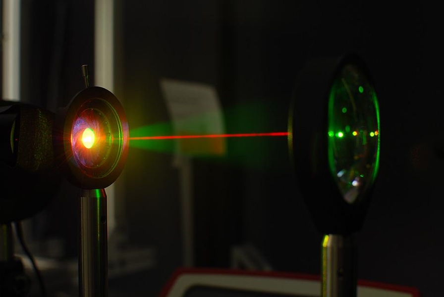
Caption:
A laser beam is used in the lab to test the gold-hyperdoped sample of silicon to confirm its infrared-sensitive properties.
Credits:
Photo courtesy of the researchers
Related Topics
Related Articles