The making of three-dimensional nanostructured materials — ones that have distinctive shapes and structures at scales of a few billionths of a meter — has become a fertile area of research, producing materials that are useful for electronics, photonics, phononics and biomedical devices. But the methods of making such materials have been limited in the 3-D complexity they can produce. Now, an MIT team has found a way to produce more complicated structures by using a blend of current "top-down" and "bottom-up" approaches.
The work is described in a paper published in June in the journal Nano Letters, co-authored by postdoc Chih-Hao Chang; George Barbastathis, the Singapore Research Professor of Optics and Professor of Mechanical Engineering; and six MIT graduate students.
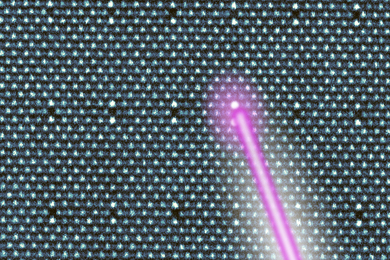
One approach to making three-dimensional nanostructures — a top-down approach — is called phase-shift lithography, in which a two-dimensional mask shapes the intensity of light shining onto a layer of photoresist material (in the same way a photographic negative controls the amount of light reaching different areas of a print). The photoresist is altered only in the areas reached by the light. However, this approach requires very precisely manufactured phase masks, which are expensive and time-consuming to make.
Another method — a bottom-up approach — is to use self-assembling colloidal nanoparticles that form themselves into certain energetically favorable close-packed arrangements. These can then be used as a mask for physical deposition methods, such as vapor deposition, or etching of the surface, to produce 2-D structures, just as a stencil can be used to control where paint reaches a surface. But these methods are slow and limited by defects that can form in the self-assembly process, so although they can be used for the fabrication of 3-D structures, this is made difficult because any defects propagate through the layers.
"We do a little bit of both," Chang says. "We took a chemist's method and added in a flavor of engineering."
The new method is a hybrid in which the self-assembled array is produced directly on a substrate material, performing the function of a mask for the lithography process. The individual nanoparticles that assemble on the surface each act as tiny lenses, focusing the beam into an intensity pattern determined by their arrangement on the surface. The method, the authors say in their paper, "can be implemented as a novel technique to fabricate complex 3-D nanostructures in all fields of nanoscale research."
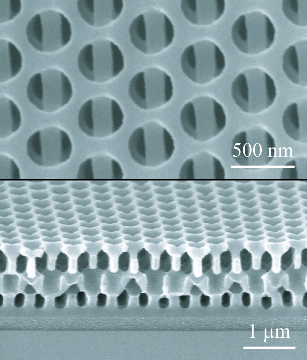
Depending on the shapes and arrangements of the tiny glass beads they use for the self-assembly part of the process, it is possible to create a great variety of structures, "from holes to higher-density posts, rings, flowery structures, all using the exact same system," Chang says. "It's a very simple way to make 3-D nanostructures, and probably the cheapest way right now. You can use it for many things."
Team members, whose specialty is in optics, say the first structures they plan to make are photonic crystals, whose structure can manipulate the behavior of light beams passing through them. But the method can also be used to make phononic materials, which control waves of heat or sound, or even to make filters with precisely controlled porosity, which might have biomedical applications.
John Rogers SM '92, PhD '95, a professor of materials science and engineering and professor of chemistry at the University of Illinois at Urbana-Champaign who was not involved in this work, says these MIT researchers have found "a remarkably simple way to do a very hard thing in nanofabrication, i.e., to create large-scale, three-dimensional nanostructures with useful shapes."
Rogers says, "The experimental simplicity, and the resulting access to structures that would be difficult or impossible to achieve in other ways, suggest that the approach will be useful for many fields of application, ranging from photonic crystals to engineered filter membranes and others."
The work is described in a paper published in June in the journal Nano Letters, co-authored by postdoc Chih-Hao Chang; George Barbastathis, the Singapore Research Professor of Optics and Professor of Mechanical Engineering; and six MIT graduate students.
One approach to making three-dimensional nanostructures — a top-down approach — is called phase-shift lithography, in which a two-dimensional mask shapes the intensity of light shining onto a layer of photoresist material (in the same way a photographic negative controls the amount of light reaching different areas of a print). The photoresist is altered only in the areas reached by the light. However, this approach requires very precisely manufactured phase masks, which are expensive and time-consuming to make.
Another method — a bottom-up approach — is to use self-assembling colloidal nanoparticles that form themselves into certain energetically favorable close-packed arrangements. These can then be used as a mask for physical deposition methods, such as vapor deposition, or etching of the surface, to produce 2-D structures, just as a stencil can be used to control where paint reaches a surface. But these methods are slow and limited by defects that can form in the self-assembly process, so although they can be used for the fabrication of 3-D structures, this is made difficult because any defects propagate through the layers.
"We do a little bit of both," Chang says. "We took a chemist's method and added in a flavor of engineering."
The new method is a hybrid in which the self-assembled array is produced directly on a substrate material, performing the function of a mask for the lithography process. The individual nanoparticles that assemble on the surface each act as tiny lenses, focusing the beam into an intensity pattern determined by their arrangement on the surface. The method, the authors say in their paper, "can be implemented as a novel technique to fabricate complex 3-D nanostructures in all fields of nanoscale research."
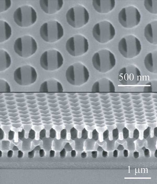
Depending on the shapes and arrangements of the tiny glass beads they use for the self-assembly part of the process, it is possible to create a great variety of structures, "from holes to higher-density posts, rings, flowery structures, all using the exact same system," Chang says. "It's a very simple way to make 3-D nanostructures, and probably the cheapest way right now. You can use it for many things."
Team members, whose specialty is in optics, say the first structures they plan to make are photonic crystals, whose structure can manipulate the behavior of light beams passing through them. But the method can also be used to make phononic materials, which control waves of heat or sound, or even to make filters with precisely controlled porosity, which might have biomedical applications.
John Rogers SM '92, PhD '95, a professor of materials science and engineering and professor of chemistry at the University of Illinois at Urbana-Champaign who was not involved in this work, says these MIT researchers have found "a remarkably simple way to do a very hard thing in nanofabrication, i.e., to create large-scale, three-dimensional nanostructures with useful shapes."
Rogers says, "The experimental simplicity, and the resulting access to structures that would be difficult or impossible to achieve in other ways, suggest that the approach will be useful for many fields of application, ranging from photonic crystals to engineered filter membranes and others."