Ask a smart home device for the weather forecast, and it takes several seconds for the device to respond. One reason this latency occurs is because connected devices don’t have enough memory or power to store and run the enormous machine-learning models needed for the device to understand what a user is asking of it. The model is stored in a data center that may be hundreds of miles away, where the answer is computed and sent to the device.
MIT researchers have created a new method for computing directly on these devices, which drastically reduces this latency. Their technique shifts the memory-intensive steps of running a machine-learning model to a central server where components of the model are encoded onto light waves.
The waves are transmitted to a connected device using fiber optics, which enables tons of data to be sent lightning-fast through a network. The receiver then employs a simple optical device that rapidly performs computations using the parts of a model carried by those light waves.
This technique leads to more than a hundredfold improvement in energy efficiency when compared to other methods. It could also improve security, since a user’s data do not need to be transferred to a central location for computation.
This method could enable a self-driving car to make decisions in real-time while using just a tiny percentage of the energy currently required by power-hungry computers. It could also allow a user to have a latency-free conversation with their smart home device, be used for live video processing over cellular networks, or even enable high-speed image classification on a spacecraft millions of miles from Earth.
“Every time you want to run a neural network, you have to run the program, and how fast you can run the program depends on how fast you can pipe the program in from memory. Our pipe is massive — it corresponds to sending a full feature-length movie over the internet every millisecond or so. That is how fast data comes into our system. And it can compute as fast as that,” says senior author Dirk Englund, an associate professor in the Department of Electrical Engineering and Computer Science (EECS) and member of the MIT Research Laboratory of Electronics.
Joining Englund on the paper is lead author and EECS grad student Alexander Sludds; EECS grad student Saumil Bandyopadhyay, Research Scientist Ryan Hamerly, as well as others from MIT, the MIT Lincoln Laboratory, and Nokia Corporation. The research is published today in Science.
Lightening the load
Neural networks are machine-learning models that use layers of connected nodes, or neurons, to recognize patterns in datasets and perform tasks, like classifying images or recognizing speech. But these models can contain billions of weight parameters, which are numeric values that transform input data as they are processed. These weights must be stored in memory. At the same time, the data transformation process involves billions of algebraic computations, which require a great deal of power to perform.
The process of fetching data (the weights of the neural network, in this case) from memory and moving them to the parts of a computer that do the actual computation is one of the biggest limiting factors to speed and energy efficiency, says Sludds.
“So our thought was, why don’t we take all that heavy lifting — the process of fetching billions of weights from memory — move it away from the edge device and put it someplace where we have abundant access to power and memory, which gives us the ability to fetch those weights quickly?” he says.
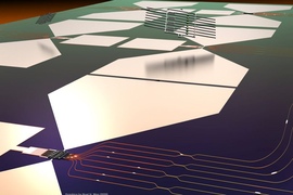
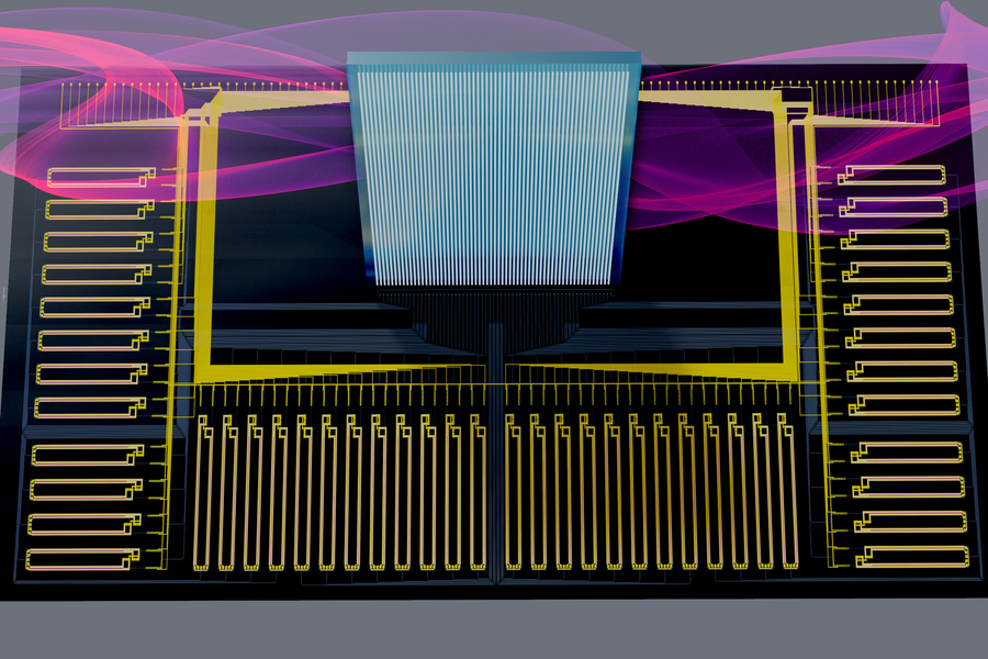
The neural network architecture they developed, Netcast, involves storing weights in a central server that is connected to a novel piece of hardware called a smart transceiver. This smart transceiver, a thumb-sized chip that can receive and transmit data, uses technology known as silicon photonics to fetch trillions of weights from memory each second.
It receives weights as electrical signals and imprints them onto light waves. Since the weight data are encoded as bits (1s and 0s) the transceiver converts them by switching lasers; a laser is turned on for a 1 and off for a 0. It combines these light waves and then periodically transfers them through a fiber optic network so a client device doesn’t need to query the server to receive them.
“Optics is great because there are many ways to carry data within optics. For instance, you can put data on different colors of light, and that enables a much higher data throughput and greater bandwidth than with electronics,” explains Bandyopadhyay.
Trillions per second
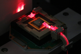
Once the light waves arrive at the client device, a simple optical component known as a broadband “Mach-Zehnder” modulator uses them to perform super-fast, analog computation. This involves encoding input data from the device, such as sensor information, onto the weights. Then it sends each individual wavelength to a receiver that detects the light and measures the result of the computation.
The researchers devised a way to use this modulator to do trillions of multiplications per second, which vastly increases the speed of computation on the device while using only a tiny amount of power.
“In order to make something faster, you need to make it more energy efficient. But there is a trade-off. We’ve built a system that can operate with about a milliwatt of power but still do trillions of multiplications per second. In terms of both speed and energy efficiency, that is a gain of orders of magnitude,” Sludds says.
They tested this architecture by sending weights over an 86-kilometer fiber that connects their lab to MIT Lincoln Laboratory. Netcast enabled machine-learning with high accuracy — 98.7 percent for image classification and 98.8 percent for digit recognition — at rapid speeds.
“We had to do some calibration, but I was surprised by how little work we had to do to achieve such high accuracy out of the box. We were able to get commercially relevant accuracy,” adds Hamerly.
Moving forward, the researchers want to iterate on the smart transceiver chip to achieve even better performance. They also want to miniaturize the receiver, which is currently the size of a shoe box, down to the size of a single chip so it could fit onto a smart device like a cell phone.
“Using photonics and light as a platform for computing is a really exciting area of research with potentially huge implications on the speed and efficiency of our information technology landscape,” says Euan Allen, a Royal Academy of Engineering Research Fellow at the University of Bath, who was not involved with this work. “The work of Sludds et al. is an exciting step toward seeing real-world implementations of such devices, introducing a new and practical edge-computing scheme whilst also exploring some of the fundamental limitations of computation at very low (single-photon) light levels.”
The research is funded, in part, by NTT Research, the National Science Foundation, the Air Force Office of Scientific Research, the Air Force Research Laboratory, and the Army Research Office.