Researchers have discovered a novel way to perform “general inverse design” with reasonably high accuracy. This breakthrough paves the way for further development of a burgeoning and fast-moving field that could eventually enable the use of machine learning to accurately identify materials based on a desired set of user-defined properties. This could be revolutionary for materials science and have vast industrial benefits and use cases.
The work was led by researchers from the Low Energy Electronic Systems (LEES) interdisciplinary research group at Singapore-MIT Alliance for Research and Technology (SMART), MIT’s research enterprise in Singapore, together with collaborators at MIT, National University of Singapore, and Nanyang Technological University.
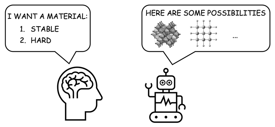
A key challenge in materials science and research has been the long-desired ability to create a material or compound with a specific set of characteristics and properties in order to suit a particular application or use case. To tackle this problem, researchers have traditionally employed materials screening via materials-property databases, which has led to the discovery of a limited number of compounds with user-defined functional properties. However, even with high-performance computing, the computational cost of the necessary calculations is high, prohibiting an exhaustive search of the theoretical materials space. Consequently, there is a pressing need for an alternative method that can make this process of “materials prospecting” more comprehensive and efficient.
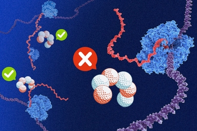
Enter inverse design. As the name suggests, the concept of inverse design reverses the conventional design process, allowing new materials and compounds to be “reverse-engineered” simply by inputting a set of desired properties and characteristics and then using an optimization algorithm to generate a predicted solution. The recent advent of inverse design has been of particular interest in the field of photonics, which is increasingly turning to unconventional technologies to circumvent inherent challenges associated with designing increasingly smaller yet more powerful devices. Current methods involve traditional design, in which a designer conceives of a fixed shape or structure as a starting point. This process is labor-intensive and excludes a wide range of other devices with different shapes or structures from consideration, some of which may have more potential than traditional shapes or structures.
Inverse design eliminates this problem and instead allows for the fabrication of devices with the most optimal or effective shape, structure, chemical composition, or other characteristics or properties. While inverse design is not new, SMART researchers have taken the technology a step further by discovering a viable method of “general” inverse design, in which inverse design capability is not limited to a particular set of elements or crystal structure, but is able to access a diversity of elements and crystal structures.
This breakthrough is outlined in a paper entitled “An invertible crystallographic representation for general inverse design of inorganic crystals with targeted properties,” recently published in the journal Matter. In the research, the team demonstrates a framework for general (both composition- and structure-varying) inverse design of inorganic crystals, called FTCP (Fourier-Transformed Crystal Properties), that allows for inverse design of crystals with user-specified properties through sampling, decoding, and post-processing. Even more promisingly, the researchers show that FTCP is able to design new crystalline materials that are dissimilar from known structures — a significant development in the exploration of this nascent technology with potentially revolutionary implications for materials science and industrial applications.
The algorithm developed by SMART researchers trains on more than 50,000 compounds in a materials database, then learns and generalizes the complex relationships between chemistry, structure, and properties in order to predict novel compounds or materials that possess user-targeted characteristics. The algorithm predicts materials with target formation energies, bandgaps, and thermoelectric power factors, and validates these predictions with simulations through density functional theory, in turn demonstrating a reasonable degree of accuracy.
“This is an incredibly exciting development for the field of materials research. Materials science researchers now have an effective and comprehensive tool that allows them to discover and create new compounds and materials by simply inputting the desired characteristics,” says Tonio Buonassisi, principal investigator at LEES and professor of mechanical engineering at MIT.
S. Isaac P. Tian, NUS graduate student and co-first author on the paper, adds “In the next step of this journey, an important milestone will be to refine the algorithm to be able to better predict stability and manufacturability. These are exciting challenges that the SMART team is currently working on with collaborators in Singapore and globally.”
Zekun Ren, lead author and postdoc at LEES, says “The aim of finding more effective and efficient ways to create materials or compounds with user-defined properties has long been the focus of materials science researchers. Our work demonstrates a viable solution that goes beyond specialized inverse design, allowing researchers to explore potential materials of varying composition and structure and thus enabling the creation of a much wider range of compounds. This is a pioneering example of successful general inverse design, and we hope to build on this success in further research efforts.”
The research is carried out by SMART and supported by the National Research Foundation (NRF) Singapore under its Campus for Research Excellence and Technological Enterprise (CREATE) program.
SMART’s LEES interdisciplinary research group is creating new integrated circuit technologies that result in increased functionality, lower power consumption, and higher performance for electronic systems. These integrated circuits of the future will impact applications in wireless communications, power electronics, LED lighting, and displays. LEES has a vertically-integrated research team possessing expertise in materials, devices, and circuits, comprising multiple individuals with professional experience within the semiconductor industry. This ensures that the research is targeted to meet the needs of the semiconductor industry, both within Singapore and globally.
SMART was established by MIT and the NRF in 2007. SMART is the first entity in CREATE developed by NRF. SMART serves as an intellectual and innovation hub for research interactions between MIT and Singapore, undertaking cutting-edge research in areas of interest to both parties. SMART currently comprises an Innovation Center and five interdisciplinary research groups: Antimicrobial Resistance, Critical Analytics for Manufacturing Personalized-Medicine, Disruptive and Sustainable Technologies for Agricultural Precision, Future Urban Mobility, and LEES.