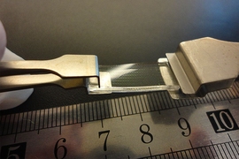
Spectrometers — devices that distinguish different wavelengths of light and are used to determine the chemical composition of everything from laboratory materials to distant stars — are large devices with six-figure price tags, and tend to be found in large university and industry labs or observatories.
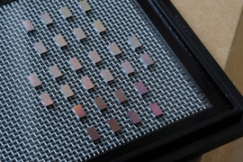
A new advance by researchers at MIT could make it possible to produce tiny spectrometers that are just as accurate and powerful but could be mass produced using standard chip-making processes. This approach could open up new uses for spectrometry that previously would have been physically and financially impossible.
The invention is described today in the journal Nature Communications, in a paper by MIT associate professor of materials science and engineering Juejun Hu, doctoral student Derek Kita, research assistant Brando Miranda, and five others.
The researchers say this new approach to making spectrometers on a chip could provide major advantages in performance, size, weight, and power consumption, compared to current instruments.
Other groups have tried to make chip-based spectrometers, but there is a built-in challenge: A device’s ability to spread out light based on its wavelength, using any conventional optical system, is highly dependent on the device’s size. “If you make it smaller, the performance degrades,” Hu says.
Another type of spectrometer uses a mathematical approach called a Fourier transform. But these devices are still limited by the same size constraint — long optical paths are essential to attaining high performance. Since high-performance devices require long, tunable optical path lengths, miniaturized spectrometers have traditionally been inferior compared to their benchtop counterparts.
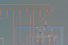
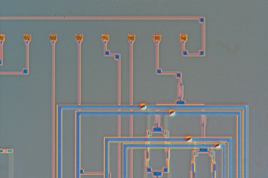
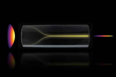
Instead, “we used a different technique,” says Kita. Their system is based on optical switches, which can instantly flip a beam of light between the different optical pathways, which can be of different lengths. These all-electronic optical switches eliminate the need for movable mirrors, which are required in the current versions, and can easily be fabricated using standard chip-making technology.
By eliminating the moving parts, Kita says, “there’s a huge benefit in terms of robustness. You could drop it off the table without causing any damage.”
By using path lengths in power-of-two increments, these lengths can be combined in different ways to replicate an exponential number of discrete lengths, thus leading to a potential spectral resolution that increases exponentially with the number of on-chip optical switches. It’s the same principle that allows a balance scale to accurately measure a broad range of weights by combining just a small number of standard weights.
As a proof of concept, the researchers contracted an industry-standard semiconductor manufacturing service to build a device with six sequential switches, producing 64 spectral channels, with built-in processing capability to control the device and process its output. By expanding to 10 switches, the resolution would jump to 1,024 channels. They designed the device as a plug-and-play unit that could be easily integrated with existing optical networks.
The team also used new machine-learning techniques to reconstruct detailed spectra from a limited number of channels. The method they developed works well to detect both broad and narrow spectral peaks, Kita says. They were able to demonstrate that its performance did indeed match the calculations, and thus opens up a wide range of potential further development for various applications.
The researchers say such spectrometers could find applications in sensing devices, materials analysis systems, optical coherent tomography in medical imaging, and monitoring the performance of optical networks, upon which most of today’s digital networks rely. Already, the team has been contacted by some companies interested in possible uses for such microchip spectrometers, with their promise of huge advantages in size, weight, and power consumption, Kita says. There is also interest in applications for real-time monitoring of industrial processes, Hu adds, as well as for environmental sensing for industries such as oil and gas.
This work “is a very interesting approach, as it enables realizing a high-resolution spectrometer on a small footprint,” says Gunther Roelkens, a professor at Ghent University in Belgium, who was not connected to this research. “This device enables applications such as on-chip spectroscopic sensors, which is a hot research topic.”
“The challenge for future research will be to extend the wavelength coverage while maintaining the same resolution,” Roelkens adds. “Also, addressing different wavelength bands will enable many new applications.”
The team also included MIT undergraduate David Favela, graduate student Jérôme Michon, former postdoc Hongtao Lin, research scientist Tian Gu, and staff member David Bono. The research was supported by the National Science Foundation, MIT SENSE.nano, the U.S. Department of Energy, and the Saks Kavanaugh Foundation.
