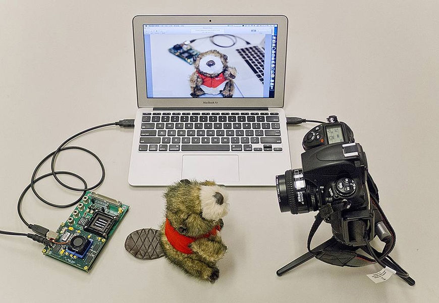
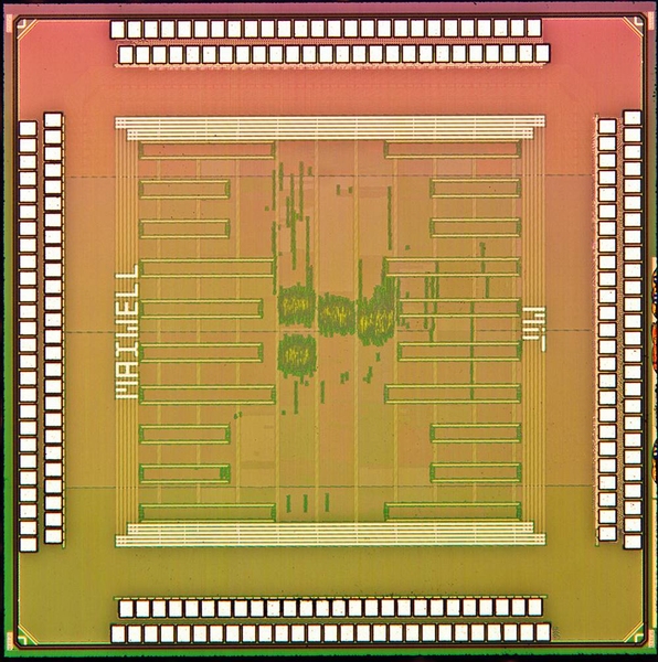
The chip, built by a team at MIT’s Microsystems Technology Laboratory, can perform tasks such as creating more realistic or enhanced lighting in a shot without destroying the scene’s ambience, in just a fraction of a second. The technology could be integrated with any smartphone, tablet computer or digital camera.
Existing computational photography systems tend to be software applications that are installed onto cameras and smartphones. However, such systems consume substantial power, take a considerable amount of time to run, and require a fair amount of knowledge on the part of the user, says the paper’s lead author, Rahul Rithe, a graduate student in MIT’s Department of Electrical Engineering and Computer Science.
“We wanted to build a single chip that could perform multiple operations, consume significantly less power compared to doing the same job in software, and do it all in real time,” Rithe says. He developed the chip with Anantha Chandrakasan, the Joseph F. and Nancy P. Keithley Professor of Electrical Engineering, fellow graduate student Priyanka Raina, research scientist Nathan Ickes and undergraduate Srikanth Tenneti.
One such task, known as High Dynamic Range (HDR) imaging, is designed to compensate for limitations on the range of brightness that can be recorded by existing digital cameras, to capture pictures that more accurately reflect the way we perceive the same scenes with our own eyes.
To do this, the chip’s processor automatically takes three separate “low dynamic range” images with the camera: a normally exposed image, an overexposed image capturing details in the dark areas of the scene, and an underexposed image capturing details in the bright areas. It then merges them to create one image capturing the entire range of brightness in the scene, Rithe says.
Software-based systems typically take several seconds to perform this operation, while the chip can do it in a few hundred milliseconds on a 10-megapixel image. This means it is even fast enough to apply to video, Ickes says. The chip consumes dramatically less power than existing CPUs and GPUs while performing the operation, he adds.
Another task the chip can carry out is to enhance the lighting in a darkened scene more realistically than conventional flash photography. “Typically when taking pictures in a low-light situation, if we don’t use flash on the camera we get images that are pretty dark and noisy, and if we do use the flash we get bright images but with harsh lighting, and the ambience created by the natural lighting in the room is lost,” Rithe says.
So in this instance the processor takes two images, one with a flash and one without. It then splits both into a base layer, containing just the large-scale features within the shot, and a detailed layer. Finally, it merges the two images, preserving the natural ambience from the base layer of the nonflash shot, while extracting the details from the picture taken with the flash.
To remove unwanted features from the image, such as noise — the unexpected variations in color or brightness created by digital cameras — the system blurs any undesired pixel with its surrounding neighbors, so that it matches those around it. In conventional filtering, however, this means even those pixels at the edges of objects are also blurred, which results in a less detailed image.
But by using what is called a bilateral filter, the researchers are able to preserve these outlines, Rithe says. That is because bilateral filters will only blur pixels with their neighbors if they have been assigned a similar brightness value. Since any objects within the image are likely to have a very different level of brightness than that of their background, this prevents the system from blurring across any edges, he says.
To perform each of these tasks, the chip’s processing unit uses a method of organizing and storing data called a bilateral grid. The image is first divided into smaller blocks. For each block, a histogram is then created. This results in a 3-D representation of the image, with the x and y axes representing the position of the block, and the brightness histogram representing the third dimension.
This makes it easy for the filter to avoid blurring across edges, since pixels with different brightness levels are separated in this third axis in the grid structure, no matter how close together they are in the image itself.
The algorithms implemented on the chip are inspired by the computational photography work of professor of computer science and engineering Fredo Durand and Bill Freeman, a professor of computer science and engineering in MIT’s Computer Science and Artificial Intelligence Laboratory. With the aid of Taiwanese semiconductor manufacturer TSMC’s University Shuttle Program, the researchers have already built a working prototype of the chip using 40-nanometer CMOS technology, and integrated it into a camera and display. They will be presenting their chip at the International Solid-State Circuits Conference in San Francisco in February.
The chip offers a hardware solution to some important problems in computational photography, says Michael Cohen at Microsoft Research in Redmond, Wash. “As algorithms such as bilateral filtering become more accepted as required processing for imaging, this kind of hardware specialization becomes more keenly needed,” he says.
The power savings offered by the chip are particularly impressive, says Matt Uyttendaele, also of Microsoft Research. “All in all [it is] a nicely crafted component that can bring computational photography applications onto more energy-starved devices,” he says.
The work was funded by the Foxconn Technology Group, based in Taiwan.


