

Folding paper into shapes such as a crane or a butterfly is challenging enough for most people. Now imagine trying to fold something that's about a hundred times thinner than a human hair and then putting it to use as an electronic device.
A team of researchers led by George Barbastathis, associate professor of mechanical engineering, is developing the basic principles of "nano-origami," a new technique that allows engineers to fold nanoscale materials into simple 3-D structures. The tiny folded materials could be used as motors and capacitors, potentially leading to better computer memory storage, faster microprocessors and new nanophotonic devices.
Traditional micro- and nano-fabrication techniques such as X-ray lithography and nano-imprinting work beautifully for two-dimensional structures, and are commonly used to build microprocessors and other micro-electrical-mechanical (MEMS) devices. However, they cannot create 3-D structures.
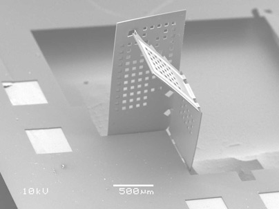
In this video, flaps of a polymer sheet are folded into a corner of a cube. An external magnetic field interacts with a current flowing through wires embedded in the sheet, causing the sheets to fold up.
Video: Nader Shaar
"A lot of what's done now is planar," says Tony Nichol, a mechanical engineering graduate student working on the project. "We want to take all of the nice tools that have been developed for 2-D and do 3-D things."
The MIT team uses conventional lithography tools to pattern 2-D materials at the nanoscale, then folds them into predetermined 3-D shapes, opening a new realm of possible applications.
Smaller, faster
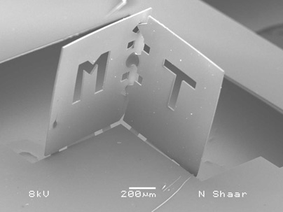
The researchers have already demonstrated a 3-D nanoscale capacitor, developed in collaboration with MIT Professor Yang Shao-Horn, which was presented at the 2005 meeting of the Electrochemical Society. The current model has only one fold but the more folds that are added, the more energy it will be able to store. Extra layers also promote faster information flow, just as the human brain's many folds allow for quicker communication between brain regions, says Nader Shaar, a mechanical engineering graduate student working on the project.
Getting the materials to fold back and forth into an accordion-like structure has been one of the researchers' biggest challenges, along with getting the faces and edges to line up accurately.
They have worked out several ways to induce the nanomaterials to fold, including:
Once the material is folded, the tricky part is getting the faces to align properly. The researchers have developed a few ways to do this successfully: one uses magnets; another involves attaching polymers to a certain spot on the faces and melting them with an electric current, sealing the two faces together.
They're still working on getting faces and edges of a folded cube to line up with nanoscale precision, but Shaar, co-supervised by associate professor of mechanical engineering Carol Livermore, has devised a promising method that uses three pairs of matching holes and protrusions to pull the edge and face into alignment.
The researchers are deep in the development phase of their nano-folded devices, but they are starting to think about how the technology could be used in the future. "We've got the core components figured out, and now we're just having fun with figuring out some applications," says Nichol.
A version of this article appeared in MIT Tech Talk on March 4, 2009 (download PDF).
A team of researchers led by George Barbastathis, associate professor of mechanical engineering, is developing the basic principles of "nano-origami," a new technique that allows engineers to fold nanoscale materials into simple 3-D structures. The tiny folded materials could be used as motors and capacitors, potentially leading to better computer memory storage, faster microprocessors and new nanophotonic devices.
Traditional micro- and nano-fabrication techniques such as X-ray lithography and nano-imprinting work beautifully for two-dimensional structures, and are commonly used to build microprocessors and other micro-electrical-mechanical (MEMS) devices. However, they cannot create 3-D structures.
In this video, flaps of a polymer sheet are folded into a corner of a cube. An external magnetic field interacts with a current flowing through wires embedded in the sheet, causing the sheets to fold up.
Video: Nader Shaar
"A lot of what's done now is planar," says Tony Nichol, a mechanical engineering graduate student working on the project. "We want to take all of the nice tools that have been developed for 2-D and do 3-D things."
The MIT team uses conventional lithography tools to pattern 2-D materials at the nanoscale, then folds them into predetermined 3-D shapes, opening a new realm of possible applications.
Smaller, faster
The researchers have already demonstrated a 3-D nanoscale capacitor, developed in collaboration with MIT Professor Yang Shao-Horn, which was presented at the 2005 meeting of the Electrochemical Society. The current model has only one fold but the more folds that are added, the more energy it will be able to store. Extra layers also promote faster information flow, just as the human brain's many folds allow for quicker communication between brain regions, says Nader Shaar, a mechanical engineering graduate student working on the project.
Getting the materials to fold back and forth into an accordion-like structure has been one of the researchers' biggest challenges, along with getting the faces and edges to line up accurately.
They have worked out several ways to induce the nanomaterials to fold, including:
- Depositing metal (usually chromium) onto the surface where you want the fold to be. This causes the material to curl upward, but it does not allow for right angles or accordion-type folds.
- Directing a beam of helium ions onto the desired fold location. The beams imprint patterns that will cause the material to fold once it's removed from the surface. High-energy beams go to the bottom of the material and cause it to fold up; ions from low-energy beams accumulate at the top of the material and make it fold down.
- Embedding gold wires in the material. A current running along the gold wires interacts with an external magnetic field, creating a Lorentz force that lifts the face. This technique is a form of directed self-assembly, where the designer provides the template and then lets the device assemble itself.
Once the material is folded, the tricky part is getting the faces to align properly. The researchers have developed a few ways to do this successfully: one uses magnets; another involves attaching polymers to a certain spot on the faces and melting them with an electric current, sealing the two faces together.
They're still working on getting faces and edges of a folded cube to line up with nanoscale precision, but Shaar, co-supervised by associate professor of mechanical engineering Carol Livermore, has devised a promising method that uses three pairs of matching holes and protrusions to pull the edge and face into alignment.
The researchers are deep in the development phase of their nano-folded devices, but they are starting to think about how the technology could be used in the future. "We've got the core components figured out, and now we're just having fun with figuring out some applications," says Nichol.
A version of this article appeared in MIT Tech Talk on March 4, 2009 (download PDF).