The huge increases in the power and capacity of computers, cell phones and communications networks in the last 40 years have been the result of ever-shrinking silicon transistors. But silicon transistors are now getting so small that they’re running up against fundamental physical limits: soon, it will be impossible to squeeze any better performance out of them. Researchers in MIT’s Microsystems Technology Laboratories, led by professor of electrical engineering Jesús del Alamo, have been investigating whether transistors made from more exotic materials can keep the processing power coming. At the International Electron Devices Meeting this week in Baltimore — the premier conference on microelectronics — they are presenting four separate papers that offer cause for hope.
Del Alamo’s group works with compound semiconductors, so called because, unlike silicon, they’re compounds of several other materials. In particular, the group works with materials that combine elements from columns III and V of the periodic table and have names like gallium arsenide and indium gallium arsenide.
Electrons travel through these so-called III-V materials much more rapidly than they do through silicon, and III-V semiconductors have been used for years in high-speed electronics, such as the devices that process data in fiber-optic networks. But according to del Alamo, the transistors in III-V optical components are “larger by several orders of magnitude” than the transistors in computer chips. Whether they can maintain their performance advantages at dramatically smaller scales is the question that del Alamo’s group is tackling.
In a computer chip, transistors serve as on-off switches that help execute logic operations — comparing two values, for instance, or performing arithmetic functions. But transistors can also be used to amplify electrical signals — as they do in transistor radios. Last year, del Alamo’s group built a III-V transistor that set a world record for high-frequency operation, meaning that it was able to amplify higher-frequency signals than any previous transistor. While that gives some sense of the transistor’s capacities, two of the four papers being presented in Baltimore assess properties of the transistor that better predict its performance as a logic element.
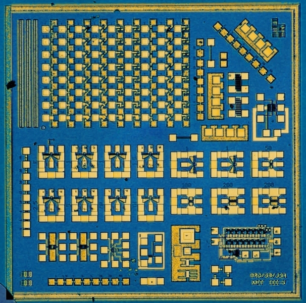
To measure those properties, del Alamo says, the group built chips with multiple transistors that were identical except for the length of their most critical element, called the gate. If a transistor is a switch, the gate is what throws it. When the gate is electrically charged, it exerts an electrostatic force on a semiconductor layer beneath it; that force is what determines whether the semiconductor can conduct electricity or not.
By comparing the performance of transistors with different gate lengths at different frequencies, del Alamo’s group was able to extract precise measurements of both the velocity of the electrons passing through the transistor and the electrostatic force that the gate exerted on the semiconductor layer.
Electron velocity, del Alamo says, is the “key velocity that is going to set the performance of a future logic switch based on these kinds of materials, and we have obtained velocities that are easily two and a half times higher than the best silicon transistors made today.” While the electrostatic force exerted by the gate was lower than the researchers had hoped, measuring it so precisely allowed del Alamo’s group to develop better physical models of III-V transistors’ behavior. On the basis of those models, del Alamo says, he believes that the gate’s performance is a “manageable problem.”
“Before the industry is willing to switch from one technology to the next technology, people in the industry would want to make sure that they were making the right bet, the right investment,” says Robert Chau, a senior fellow at chip giant Intel who has worked closely with del Alamo’s group. “So obviously, people will need to thoroughly understand the physics behind this proposed new technology. I think that’s what Professor del Alamo’s group has been doing — getting to the science of the device operation.”
The third paper is in a similar vein, a collaboration with researchers at Purdue University who have developed simulators to model the performance of III-V transistors that are even smaller than the MIT prototypes. Del Alamo’s group used its precise measurements of the prototypes’ performance to help the Purdue team calibrate its simulator. The fourth paper, however, addresses a different topic: it proposes a new design for III-V transistors that, del Alamo says, will work better at smaller scales, because it permits a thinner layer of material to separate the gate and the semiconductor material beneath it.
For all their speed, III-V semiconductors have a disadvantage as a next-generation chip material: they’re rarer, and therefore more expensive, than silicon. But while the MIT prototypes were built entirely with III-V materials, del Alamo envisions “a silicon-like technology where just under the gate … you take silicon out and stick in indium gallium arsenide. It’s a minute amount of material that is required in every transistor to make this happen.” Indeed, “III-V is not really in competition with silicon,” Chau agrees. “It still will be a silicon transistor. It’s just that you’re using this non-silicon element to make it even better.”


