New ways of squeezing out greater efficiency from solar photovoltaic cells are emerging from computer simulations and lab tests conducted by a team of physicists and engineers at MIT.
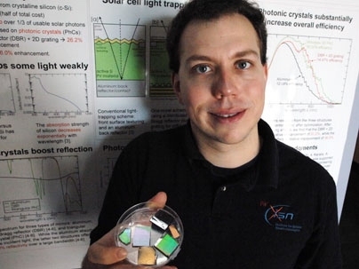
Using computer modeling and a variety of advanced chip-manufacturing techniques, they have applied an antireflection coating to the front, and a novel combination of multi-layered reflective coatings and a tightly spaced array of lines -- called a diffraction grating -- to the backs of ultrathin silicon films to boost the cells' output by as much as 50 percent.
The carefully designed layers deposited on the back of the cell cause the light to bounce around longer inside the thin silicon layer, giving it time to deposit its energy and produce an electric current. Without these coatings, light would just be reflected back out into the surrounding air, said Peter Bermel, a postdoctoral researcher in MIT's Research Laboratory of Electronics who has been working on the project.
"It's critical to ensure that any light that enters the layer travels through a long path in the silicon," Bermel said. "The issue is how far does light have to travel [in the silicon] before there's a high probability of being absorbed" and knocking loose electrons to produce an electric current.
The team began by running thousands of computer simulations in which they tried out variations in the spacing of lines in the grid, the thickness of the silicon and the number and thicknesses of reflective layers deposited on the back surface. "We use our simulation tools to optimize overall efficiency and maximize the power coming out," Bermel said.
"The simulated performance was remarkably better than any other structure, promising, for 2-micrometer-thick films, a 50 percent efficiency increase in conversion of sunlight to electricity," said Lionel Kimerling, the Thomas Lord Professor of Materials Science and Engineering, who directed the project.
The simulations were then validated by actual lab-scale tests. "The final and most important ingredient was the relentless dedication of graduate student Lirong Zeng, in the Department of Materials Science and Engineering, to refining the structure and making it," Kimerling said. "The experiments confirmed the predictions, and the results have drawn considerable industry interest."
The team will report the first reduction to practice of their findings on Dec. 2 at the Materials Research Society's annual meeting in Boston. A paper on their findings has been accepted for publication in Applied Physics Letters.
The work is just a first step toward actually producing a commercially viable, improved solar cell. That will require additional fine-tuning through continuing simulations and lab tests, and then more work on the manufacturing processes and materials. "If the solar business stays strong," Kimerling said, "implementation within the next three years is possible."
The MIT Deshpande Center selected the project for an "i-team" study to evaluate its business potential. The team analyzed the potential impact of this efficient thin solar cell technology and found significant benefits in both manufacturing and electrical power delivery, for applications ranging from remote off-grid to dedicated clean power.
And the potential for savings is great, because the high-quality silicon crystal substrates used in conventional solar cells represent about half the cost, and the thin films in this version use only about 1 percent as much silicon, Bermel said.
This project, along with other research work going on now in solar cells, has the potential to get costs down "so that it becomes competitive with grid electricity," Bermel said. While no single project is likely to achieve that goal, he said, this work is "the kind of science that needs to be explored in order to achieve that."
In addition to Kimerling, Bermel and Zeng, the work was done by John Joannopoulos, the Francis Wright Davis Professor of Physics, and by research engineer Bernard A. Alamariu, research specialist Kurt A. Broderick, both of the Microsystems Technology Laboratories; postdoctoral associate Jifeng Liu; Ching-yin Hong, former PhD student Yasha Yi, and research associate Xiaoman Duan of the Materials Processing Center. Funding was provided by the Thomas Lord Chair in Materials Science and Engineering, the MIT-MIST Initiative, the Materials Research Science and Engineering Center Program of the NSF and the Army Research Office through the Institute for Soldier Nanotechnologies.
A version of this article appeared in MIT Tech Talk on December 3, 2008 (download PDF).
