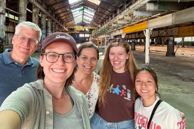
A wafer of silicon four inches in diameter and an actual microchip were among the souvenirs given to MIT parents touring the Microsystems Technology Laboratories (MTL) last Friday, appropriate mementos since the tour showed how researchers get from one to the other.
After donning special booties to avoid tracking contaminants into the laboratory, parents and others on the Family Weekend tour were shown the equipment used to create microchips and other microsystems. Most of the equipment is actually housed in separate windowed "clean rooms" along an outer corridor. Researchers within these rooms wear protective clothing from head to toe.
"In semiconductor manufacturing, a human being is the largest source of contamination we have," said Barry Farnsworth, an MTL research specialist.
Among the lab's equipment: a metal sputtering machine for depositing metal on a wafer. "We put a wafer in with a metal target above, then pump out all the air," Dr. Farnsworth said. Argon is pumped in and a plasma, or electrically charged gas, "knocks little pieces of the target off." Those pieces go onto the wafer.
Dr. Farnsworth noted that the films of material deposited onto wafers are so thin -- often less than two percent of the thickness of a human hair -- that they're difficult to measure by conventional means. One technique for doing so is to shine a laser beam at the sample, he said. "We look for changes in light to measure how thick the film is."
The tour also included a glimpse of the photolithography area, where wafers are patterned, and the diffusion area, home of another technique for depositing materials on a wafer. One of the final stops: a room where the many microdevices on a wafer are cut from it, and where wires can be added to connect a given device to a support structure that can be plugged into a computer.
MIT graduate students use the laboratory to create their own microsystems. MTL staff train them to run the machines and help them realize their ideas.
Other tours offered during Family Weekend included the Artificial Intelligence Lab, the Media Lab, and the Plasma Science and Fusion Center.
A version of this article appeared in MIT Tech Talk on October 20, 1999.


