New START.nano cohort is developing solutions in health, data storage, power, and sustainable energy
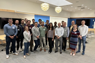
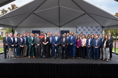
With seven new startups, MIT.nano's program for hard-tech ventures expands to more than 20 companies.
With seven new startups, MIT.nano's program for hard-tech ventures expands to more than 20 companies.
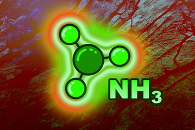
Using the Earth itself as a chemical reactor could reduce the need for fossil-fuel-powered chemical plants.
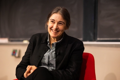
In her 2024 Dresselhaus Lecture, the Cambridge University professor of chemistry describes her work making batteries more reliable and sustainable.
As part of a high-resolution biosensing device without wires, the antennas could help researchers decode intricate electrical signals sent by cells.
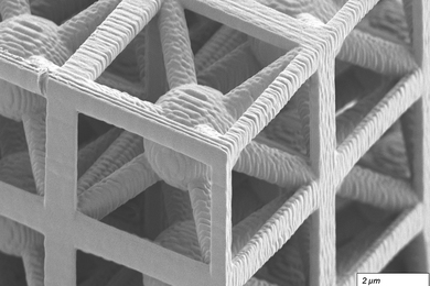
New framework advances experimental capabilities, including design and characterization, of microscale acoustic metamaterials.
A new electrode design boosts the efficiency of electrochemical reactions that turn carbon dioxide into ethylene and other products.
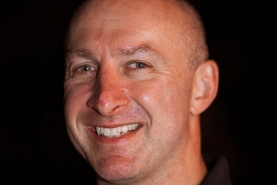
At MIT, Keselman is a lecturer, executive director, managing director, and innovator. Additionally, he is a colonel in the Air Force Reserves, board director, and startup leader.

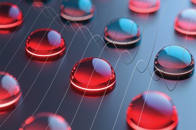
Researchers are leveraging quantum mechanical properties to overcome the limits of silicon semiconductor technology.
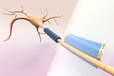
By snugly wrapping around neurons, these devices could help scientists probe subcellular regions of the brain, and might even help restore some brain function.

A new study of bubbles on electrode surfaces could help improve the efficiency of electrochemical processes that produce fuels, chemicals, and materials.
MIT and Lincoln Laboratory are among awardees of $38 million in project awards to the Northeast Microelectronics Coalition to boost U.S. chip technology innovation.
New STUDIO.nano supports artistic research and encounters within MIT.nano’s facilities.
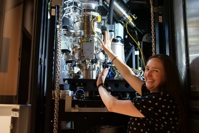
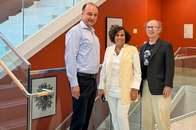
For Sarah Sterling, the new director of the Cryo-Electron Microscopy facility at MIT.nano, better planning and more communication leads to better science.
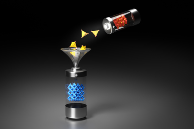
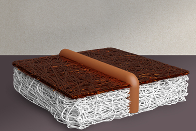
A new family of integrated rock salt-polyanion cathodes opens door to low-cost, high-energy storage.
A trailblazer in electron microscopy, Vander Sande is remembered for his dedication to teaching, service, and global collaboration.