Last semester, MIT undergraduates completed the first-ever term of coursework to be done utilizing the facilities of MIT.nano, the Institute’s new 216,000 square-foot center for nanoscale research.
The course — 3.155/6.152 (Micro/Nano Processing Technology), offered jointly by the departments of Electrical Engineering and Computer Science (EECS) and Materials Science and Engineering (DMSE) — enrolled 25 undergraduate and nine graduate students from seven different departments in fall 2019. The students learned nanofabrication by using research space and equipment throughout MIT.nano to make solar cells, MEMS cantilever beams, and microfluidic devices.
“This 2019 cohort is part of MIT’s history — the first to complete coursework through hands-on research in MIT.nano,” says Vladimir Bulović, faculty director of MIT.nano and the Fariborz Maseeh (1990) Professor in Emerging Technology. “We are thrilled to see undergraduate and graduate students from multiple disciplines honing their skills in MIT.nano cleanrooms and labs. It was great to see them innovate with tools of MIT.nano as they designed outstanding projects. We very much look forward to welcoming the next cohort of hands-on scholars.”
Co-taught by Jurgen Michel, senior research associate at DMSE, and Jorg Scholvin, assistant director for user services at MIT.nano, the course was overhauled in 2017 to become more student-driven with an added element of creativity where students get to design and build their own devices. Scholvin emphasizes the importance of teaching the students not only how to run the equipment, but how to work safely and effectively in a cleanroom and to understand the theoretical background of the fabrication equipment.
“Being able to work at and understand the nanoscale is becoming more and more essential in all science and engineering fields,” says Scholvin. “In this course, we work with students from many departments with very different scientific backgrounds and interests to give them basic skills that they can use to implement their own ideas. Then, they can go forward and adapt these processes to address higher-level, complex, interesting problems in the future.”
Learn the basics, design your own solutions
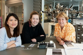
Before being set loose on their own designs, students completed two lab modules. In the first, focused on solar cells, they fabricated a silicon-based device and then tested it using the ENI Solar Frontiers tools in the third-floor MIT.nano cleanroom. The students later packaged their finished solar cells using electronic and photonic packaging tools in the fifth-floor prototyping facility. Students worked under the guidance of Anu Agarwal, principal research scientist at MIT's Microphotonics Center, and used equipment from the AIM Photonics Lab for Education and Application Prototypes toolset to connect their solar cells to circuit boards using wirebonds.
Choosing between MEMS cantilevers or microfluidic channels for the second module, students conducted wet etching of cantilever beams on the first-floor cleanroom of MIT.nano or fabricated microfluidics in the third-floor soft lithography lab. In addition to etching and fabrication, students learned about chemical and physical deposition, thermal processes, and device and materials characterization. These lab modules provide the background knowledge needed for students to apply one of these processes to their own projects.
“6.152 was a great opportunity to get first-hand nanofabrication experience combined with theoretical classroom knowledge," says Ella Richards, a junior in DMSE. "The class showcased the creative research possibilities that MIT.nano has to offer, and the resilience needed to make them a reality."
The real fun began in the final stage of the course, when students formulated their own device ideas, based on cantilevers or fluidic mixers, in a start-to-finish project. “First, the students get experience working in a cleanroom and learn the theory of processes and tools. Then, they apply their own background and interests to build and test something new,” says Scholvin. “This is when the creativity of the toolset is really driven by the students.”
Students from different departments chose different designs and projects based on their research focus. Scholvin emphasizes that this variety of work illustrates the importance of shared access to equipment. By not being dedicated to one project in one specific lab, but rather being housed at MIT.nano where any trained researcher can use it, he says, a tool can be applied to several projects in different disciplines.
Experiencing the full spectrum of fabrication
The goal, according to the instructors, is not simply tool training, but to give students exposure to the full spectrum of research in nanofabrication. The students must conceive of their own devices, pitch their ideas to the class, create CAD layouts, fabricate the device, debug the process, and test the results. And, as in any research project, they write a paper and have the opportunity to present their ideas and results to a broader technical audience.
At the conclusion of the course, prizes were awarded for the most innovative designs and the three best papers. Andison Tran, Ella Richards, and Stefan Wan were honored for their designs. Tran and Wan are majoring in chemical engineering, Richards in materials science and engineering. Kristina Greenwood, Kyle James, and Blair Anaman Williams received awards for their papers; all three are chemical engineering majors.
"I really enjoyed taking 6.152. It was the first time I was exposed to nanofabrication and I'm grateful for the amount of effort the course staff put into making what was such a new concept to me both interesting and easy to understand. I appreciated how we were given liberty to create our own devices, which brought to life all the principles and skills we learned in the class. Getting to spend time in the cleanrooms was an experience I'll never forget," says Williams, a junior in chemical engineering.
The 6.152J/3.155J students were eligible to present their projects at the Microsystems Annual Research Conference (MARC), co-sponsored by MIT.nano and Microsystems Technology Laboratories at the end of January. Five undergraduates and two graduate students from the class presented their work — Williams from chemical engineering; Abdulmalik Alghonaim, Michael Dubrovsky (graduate student), Danielle Grey-Stewart, Ella Richards, and Ava Waitz, all from DMSE; and Shubham Yadav (graduate student) from the Program in Media Arts & Sciences. Heyi Li (mechanical engineering) and Zachary Pitcher (EECS), both undergraduates, also attended the conference.
The micro/nano processing technology course will be offered again in fall 2020.