
Carbon nanotube transistors are a step closer to commercial reality, now that MIT researchers have demonstrated that the devices can be made swiftly in commercial facilities, with the same equipment used to manufacture the silicon-based transistors that are the backbone of today’s computing industry.
Carbon nanotube field-effect transistors or CNFETs are more energy-efficient than silicon field-effect transistors and could be used to build new types of three-dimensional microprocessors. But until now, they’ve existed mostly in an “artisanal” space, crafted in small quantities in academic laboratories.
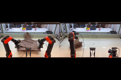
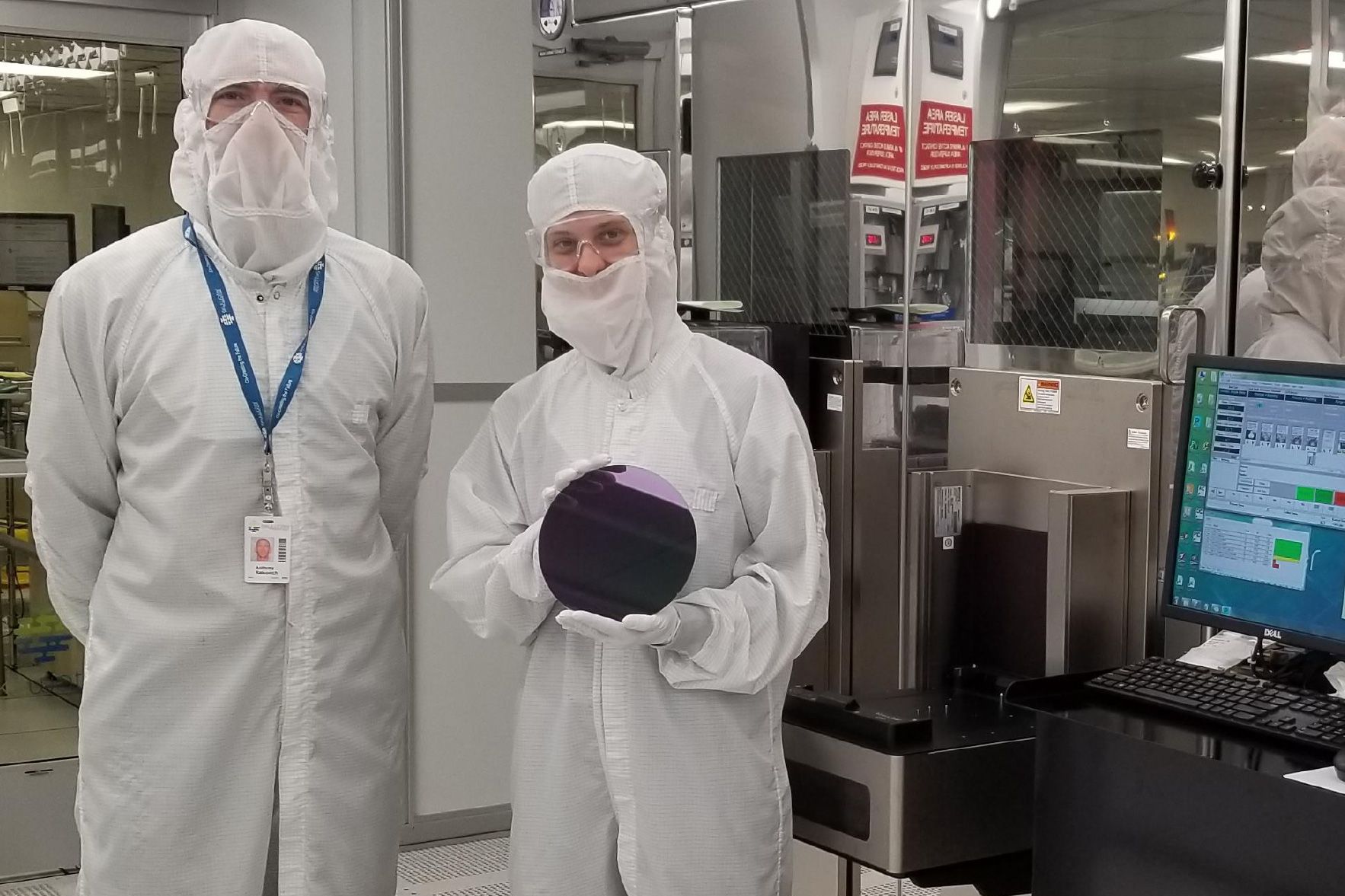
In a study published June 1 in Nature Electronics, however, scientists show how CNFETs can be fabricated in large quantities on 200-millimeter wafers that are the industry standard in computer chip design. The CNFETs were created in a commercial silicon manufacturing facility and a semiconductor foundry in the United States.
After analyzing the deposition technique used to make the CNFETs, Max Shulaker, an MIT assistant professor of electrical engineering and computer science, and his colleagues made some changes to speed up the fabrication process by more than 1,100 times compared to the conventional method, while also reducing the cost of production. The technique deposited carbon nanotubes edge to edge on the wafers, with 14,400 by 14,400 arrays CNFETs distributed across multiple wafers.
Shulaker, who has been designing CNFETs since his PhD days, says the new study represents “a giant step forward, to make that leap into production-level facilities.”
Bridging the gap between lab and industry is something that researchers “don’t often get a chance to do,” he adds. “But it’s an important litmus test for emerging technologies.”
Other MIT researchers on the study include lead author Mindy D. Bishop, a PhD student in the Harvard-MIT Health Sciences and Technology program, along with Gage Hills, Tathagata Srimani, and Christian Lau.
Solving the spaghetti problem
For decades, improvements in silicon-based transistor manufacturing have brought down prices and increased energy efficiency in computing. That trend may be nearing its end, however, as increasing numbers of transistors packed into integrated circuits do not appear to be increasing energy efficiency at historic rates.
CNFETs are an attractive alternative technology because they are “around an order of magnitude more energy efficient” than silicon-based transistors, says Shulaker.
Unlike silicon-based transistors, which are made at temperatures around 450 to 500 degrees Celsius, CNFETs also can be manufactured at near-room temperatures. “This means that you can actually build layers of circuits right on top of previously fabricated layers of circuits, to create a three-dimensional chip,” Shulaker explains. “You can’t do this with silicon-based technology, because you would melt the layers underneath.”
A 3D computer chip, which might combine logic and memory functions, is projected to “beat the performance of a state-of-the-art 2D chip made from silicon by orders of magnitude,” he says.
One of the most effective ways to build CNFETs in the lab is a method for depositing nanotubes called incubation, where a wafer is submerged in a bath of nanotubes until the nanotubes stick to the wafer’s surface.
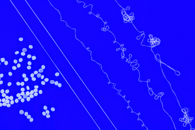
The performance of the CNFET is dictated in large part by the deposition process, says Bishop, which affects both the number of carbon nanotubes on the surface of the wafer and their orientation. They’re “either stuck onto the wafer in random orientations like cooked spaghetti or all aligned in the same direction like uncooked spaghetti still in the package,” she says.
Aligning the nanotubes perfectly in a CNFET leads to ideal performance, but alignment is difficult to obtain. “It’s really hard to lay down billions of tiny 1-nanometer diameter nanotubes in a perfect orientation across a large 200-millimeter wafer,” Bishop explains. “To put these length scales into context, it’s like trying to cover the entire state of New Hampshire in perfectly oriented dry spaghetti.”
The incubation method, while practical for industry, doesn’t align the nanotubes at all. They end up on the wafer more like cooked spaghetti, which the researchers initially didn’t think would deliver sufficiently high CNFET performance, Bishop says. After their experiments, however, she and her colleagues concluded that the simple incubation process would work to produce a CNFET that could outperform a silicon-based transistor.
CNFETs beyond the beaker
Careful observations of the incubation process showed the researchers how to alter the process to make it more viable for industrial production. For instance, they found that dry cycling, a method of intermittently drying out the submerged wafer, could dramatically reduce the incubation time — from 48 hours to 150 seconds.
Another new method called ACE (artificial concentration through evaporation) deposited small amounts of nanotube solution on a wafer instead of submerging the wafer in a tank. The slow evaporation of the solution increased the concentration of carbon nanotubes and the overall density of nanotubes deposited on the wafer.
These changes were necessary before the process could be tried on an industrial scale, Bishop says: “In our lab, we’re fine to let a wafer sit for a week in a beaker, but for a company, they don’t have that luxury.”
The “elegantly simple tests” that helped them understand and improve on the incubation method, she says, “proved really important for addressing concerns that maybe academics don’t have, but certainly industry has, when they look at setting up a new process.”
The researchers worked with Analog Devices, a commercial silicon manufacturing facility, and SkyWater Technology, a semiconductor foundry, to fabricate CNFETs using the improved method. They were able to use the same equipment that the two facilities use to make silicon-based wafers, while also ensuring that the nanotube solutions met the strict chemical and contaminant requirements of the facilities.
“We were extremely lucky to work closely with our industry collaborators and learn about their requirements and iterate our development with their input,” says Bishop, who noted that the partnership helped them develop an automated, high-volume and low-cost process.
The two facilities showed a “serious commitment to research and development and exploring the edge” of emerging technologies, Shulaker adds.
“We are excited to continue our work building out the critical infrastructure for enabling commercial market availability of CNFETs. This effort is a pivotal move to bring back manufacturing of leading-edge advanced computing to the U.S.,” said Thomas Sonderman, president of SkyWater.
The next steps, already underway, will be to build different types of integrated circuits out of CNFETs in an industrial setting and explore some of the new functions that a 3D chip could offer, he says. “The next goal is for this to transition from being academically interesting to something that will be used by folks, and I think this is a very important step in this direction.”