

As embedded intelligence is finding its way into ever more areas of our lives, fields ranging from autonomous driving to personalized medicine are generating huge amounts of data. But just as the flood of data is reaching massive proportions, the ability of computer chips to process it into useful information is stalling.
Now, researchers at Stanford University and MIT have built a new chip to overcome this hurdle. The results are published today in the journal Nature, by lead author Max Shulaker, an assistant professor of electrical engineering and computer science at MIT. Shulaker began the work as a PhD student alongside H.-S. Philip Wong and his advisor Subhasish Mitra, professors of electrical engineering and computer science at Stanford. The team also included professors Roger Howe and Krishna Saraswat, also from Stanford.
Computers today comprise different chips cobbled together. There is a chip for computing and a separate chip for data storage, and the connections between the two are limited. As applications analyze increasingly massive volumes of data, the limited rate at which data can be moved between different chips is creating a critical communication “bottleneck.” And with limited real estate on the chip, there is not enough room to place them side-by-side, even as they have been miniaturized (a phenomenon known as Moore’s Law).
To make matters worse, the underlying devices, transistors made from silicon, are no longer improving at the historic rate that they have for decades.
The new prototype chip is a radical change from today’s chips. It uses multiple nanotechnologies, together with a new computer architecture, to reverse both of these trends.
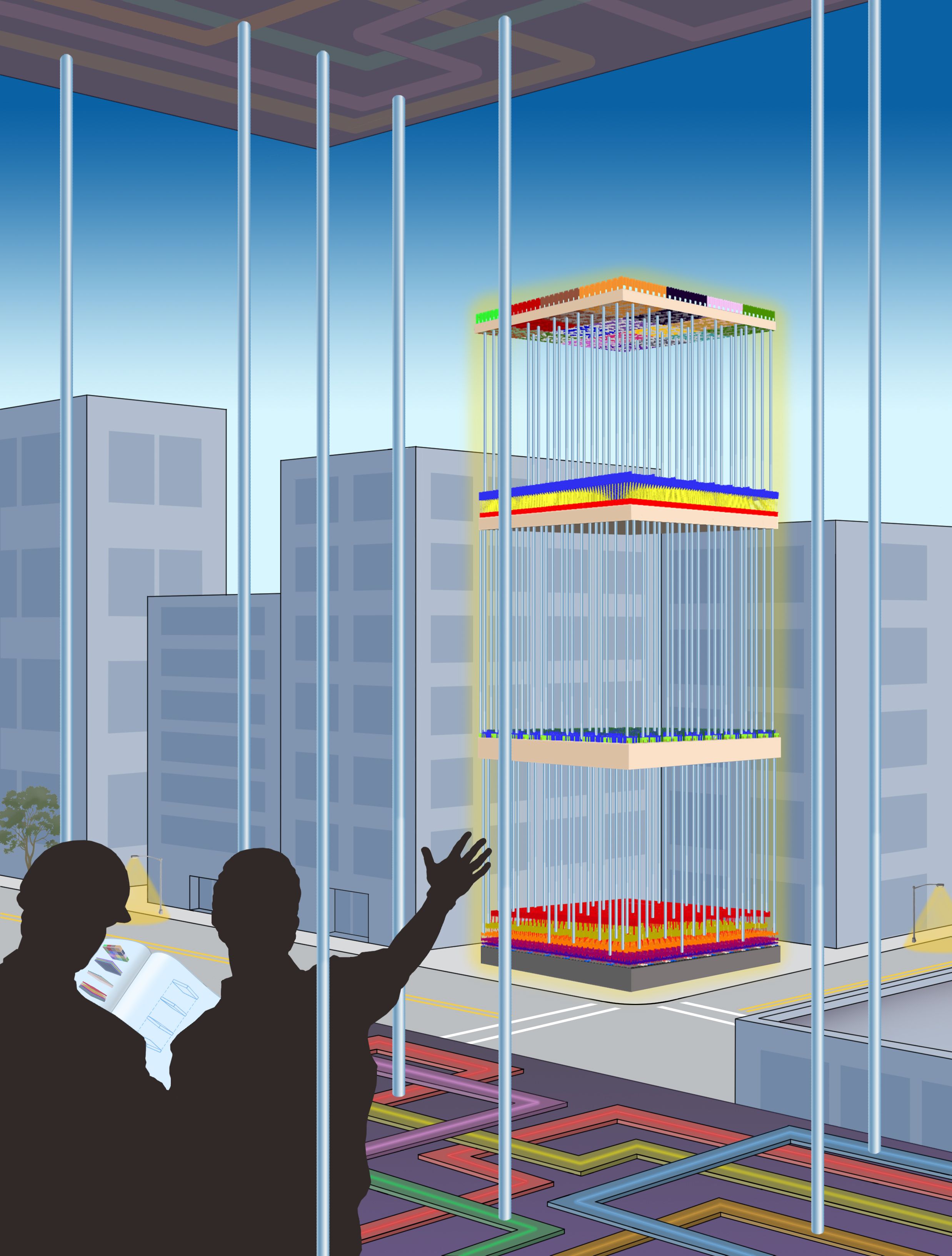
Instead of relying on silicon-based devices, the chip uses carbon nanotubes, which are sheets of 2-D graphene formed into nanocylinders, and resistive random-access memory (RRAM) cells, a type of nonvolatile memory that operates by changing the resistance of a solid dielectric material. The researchers integrated over 1 million RRAM cells and 2 million carbon nanotube field-effect transistors, making the most complex nanoelectronic system ever made with emerging nanotechnologies.
The RRAM and carbon nanotubes are built vertically over one another, making a new, dense 3-D computer architecture with interleaving layers of logic and memory. By inserting ultradense wires between these layers, this 3-D architecture promises to address the communication bottleneck.
However, such an architecture is not possible with existing silicon-based technology, according to the paper’s lead author, Max Shulaker, who is a core member of MIT’s Microsystems Technology Laboratories. “Circuits today are 2-D, since building conventional silicon transistors involves extremely high temperatures of over 1,000 degrees Celsius,” says Shulaker. “If you then build a second layer of silicon circuits on top, that high temperature will damage the bottom layer of circuits.”
The key in this work is that carbon nanotube circuits and RRAM memory can be fabricated at much lower temperatures, below 200 C. “This means they can be built up in layers without harming the circuits beneath,” Shulaker says.
This provides several simultaneous benefits for future computing systems. “The devices are better: Logic made from carbon nanotubes can be an order of magnitude more energy-efficient compared to today’s logic made from silicon, and similarly, RRAM can be denser, faster, and more energy-efficient compared to DRAM,” Wong says, referring to a conventional memory known as dynamic random-access memory.
“In addition to improved devices, 3-D integration can address another key consideration in systems: the interconnects within and between chips,” Saraswat adds.
“The new 3-D computer architecture provides dense and fine-grained integration of computating and data storage, drastically overcoming the bottleneck from moving data between chips,” Mitra says. “As a result, the chip is able to store massive amounts of data and perform on-chip processing to transform a data deluge into useful information.”
To demonstrate the potential of the technology, the researchers took advantage of the ability of carbon nanotubes to also act as sensors. On the top layer of the chip they placed over 1 million carbon nanotube-based sensors, which they used to detect and classify ambient gases.
Due to the layering of sensing, data storage, and computing, the chip was able to measure each of the sensors in parallel, and then write directly into its memory, generating huge bandwidth, Shulaker says.
Three-dimensional integration is the most promising approach to continue the technology scaling path set forth by Moore’s laws, allowing an increasing number of devices to be integrated per unit volume, according to Jan Rabaey, a professor of electrical engineering and computer science at the University of California at Berkeley, who was not involved in the research.
“It leads to a fundamentally different perspective on computing architectures, enabling an intimate interweaving of memory and logic,” Rabaey says. “These structures may be particularly suited for alternative learning-based computational paradigms such as brain-inspired systems and deep neural nets, and the approach presented by the authors is definitely a great first step in that direction.”
“One big advantage of our demonstration is that it is compatible with today’s silicon infrastructure, both in terms of fabrication and design,” says Howe.
“The fact that this strategy is both CMOS [complementary metal-oxide-semiconductor] compatible and viable for a variety of applications suggests that it is a significant step in the continued advancement of Moore’s Law,” says Ken Hansen, president and CEO of the Semiconductor Research Corporation, which supported the research. “To sustain the promise of Moore’s Law economics, innovative heterogeneous approaches are required as dimensional scaling is no longer sufficient. This pioneering work embodies that philosophy.”
The team is working to improve the underlying nanotechnologies, while exploring the new 3-D computer architecture. For Shulaker, the next step is working with Massachusetts-based semiconductor company Analog Devices to develop new versions of the system that take advantage of its ability to carry out sensing and data processing on the same chip.
So, for example, the devices could be used to detect signs of disease by sensing particular compounds in a patient’s breath, says Shulaker.
“The technology could not only improve traditional computing, but it also opens up a whole new range of applications that we can target,” he says. “My students are now investigating how we can produce chips that do more than just computing.”
“This demonstration of the 3-D integration of sensors, memory, and logic is an exceptionally innovative development that leverages current CMOS technology with the new capabilities of carbon nanotube field–effect transistors,” says Sam Fuller, CTO emeritus of Analog Devices, who was not involved in the research. “This has the potential to be the platform for many revolutionary applications in the future.”
This work was funded by the Defense Advanced Research Projects Agency, the National Science Foundation, Semiconductor Research Corporation, STARnet SONIC, and member companies of the Stanford SystemX Alliance.