
Since the 1960s, computer chips have been built using a process called photolithography. But in the past five years, chip features have gotten smaller than the wavelength of light, which has required some ingenious modifications of photolithographic processes. Keeping up the rate of circuit miniaturization that we’ve come to expect — as predicted by Moore’s Law — will eventually require new manufacturing techniques.
Block copolymers, molecules that spontaneously self-assemble into useful shapes, are one promising alternative to photolithography. In a new paper in the journal Nature Communications, MIT researchers describe the first technique for stacking layers of block-copolymer wires such that the wires in one layer naturally orient themselves perpendicularly to those in the layer below.
The ability to easily produce such “mesh structures” could make self-assembly a much more practical way to manufacture memory, optical chips, and even future generations of computer processors.
“There is previous work on fabricating a mesh structure — for example our work,” says Amir Tavakkoli, a postdoc in MIT’s Research Laboratory of Electronics and one of three first authors on the new paper. “We used posts that we had fabricated by electron-beam lithography, which is time consuming. But here, we don’t use the electron-beam lithography. We use the first layer of block copolymer as a template to self-assemble another layer of block copolymer on top of it.”
Tavakkoli’s co-first-authors on the paper are Sam Nicaise, a graduate student in electrical engineering, and Karim Gadelrab, a graduate student in materials science and engineering. The senior authors are Alfredo Alexander-Katz, the Walter Henry Gale Associate Professor of Materials Science and Engineering; Caroline Ross, the Toyota Professor of Materials Science and Engineering; and Karl Berggren, a professor of electrical engineering.
Unhappy couples
Polymers are long molecules made from basic molecular units strung into chains. Plastics are polymers, and so are biological molecules like DNA and proteins. A copolymer is a polymer made by joining two different polymers.
In a block copolymer, the constituent polymers are chosen so that they’re chemically incompatible with each other. It’s their attempts to push away from each other — both within a single polymer chain and within a polymer film — that causes them to self-organize.
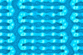
In the MIT researchers’ case, one of the constituent polymers is carbon-based, the other silicon-based. In their efforts to escape the carbon-based polymer, the silicon-based polymers fold in on themselves, forming cylinders with loops of silicon-based polymer on the inside and the other polymer bristling on the outside. When the cylinders are exposed to an oxygen plasma, the carbon-based polymer burns away and the silicon oxidizes, leaving glass-like cylinders attached to a base.
To assemble a second layer of cylinders, the researchers simply repeat the process, albeit using copolymers with slightly different chain lengths. The cylinders in the new layer naturally orient themselves perpendicularly to those in the first.
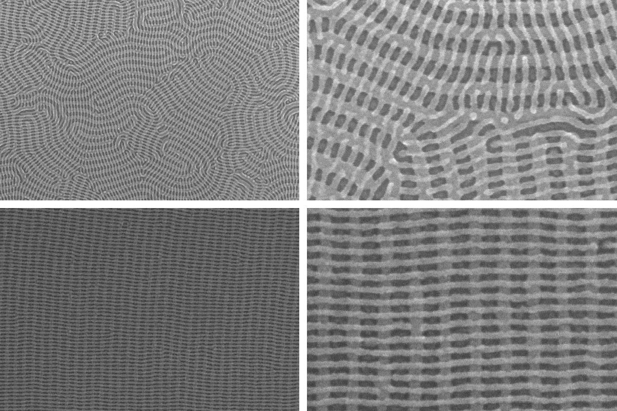
Chemically treating the surface on which the first group of cylinders are formed will cause them to line up in parallel rows. In that case, the second layer of cylinders will also form parallel rows, perpendicular to those in the first.
But if the cylinders in the bottom layer are allowed to form haphazardly, snaking out into elaborate, looping patterns, the cylinders in the second layer will maintain their relative orientation, creating their own elaborate, but perpendicular, patterns.
The orderly mesh structure is the one that has the most obvious applications, but the disorderly one is perhaps the more impressive technical feat. “That’s the one the materials scientists are excited about,” Nicaise says.
Whys and wherefores
Glass-like wires are not directly useful for electronic applications, but it might be possible to seed them with other types of molecules, which would make them electronically active, or to use them as a template for depositing other materials. The researchers hope that they can reproduce their results with more functional polymers. To that end, they had to theoretically characterize the process that yielded their results. “We use computer simulations to understand the key parameters controlling the polymer orientation,” Gadelrab says.
What they found was that the geometry of the cylinders in the bottom layer limited the possible orientations of the cylinders in the upper layer. If the walls of the lower cylinders are too steep to permit the upper cylinders from fitting in comfortably, the upper cylinders will try to find a different orientation.
It’s also important that the upper and lower layers have only weak chemical interactions. Otherwise, the upper cylinders will try to stack themselves on top of the lower ones like logs on a pile.
Both of these properties — cylinder geometry and chemical interaction — can be predicted from the physics of polymer molecules. So it should be possible to identify other polymers that will exhibit the same behavior.
According to Patrick Theofanis, an engineer at the chip manufacturer Intel, the nanocylinders themselves are less interesting than the spaces between them. “In general, the ability to pattern square holes is very useful for us,” he says.
“If you think of the back end of our chips, we have the back-end wiring, and then you have the interconnect layers between those back-end metal layers, and that’s where you’d like to be able to punch through holes and connect one layer to the next one. It’s an attractive technology because the aspect ratio is very tunable in the way that they’ve done their scheme.”
The research was funded by the National Science Foundation and the Taiwan Semiconductor Manufacturing Corporation.