

Researchers at MIT have developed a new approach to creating the complex array of wires and connections on microchips, using a system of self-assembling polymers. The work could eventually lead to a way of making more densely packed components on memory chips and other devices.
The new method — developed by MIT visiting doctoral student Amir Tavakkoli of the National University of Singapore, along with two other graduate students and three professors in MIT’s departments of Electrical Engineering and Computer Science (EECS) and Materials Science and Engineering (DMSE) — is described in a paper to be published this August in the journal Advanced Materials; the paper is available online now.
The process is closely related to a method the same team described last month in a paper in Science, which makes it possible to produce three-dimensional configurations of wires and connections using a similar system of self-assembling polymers.
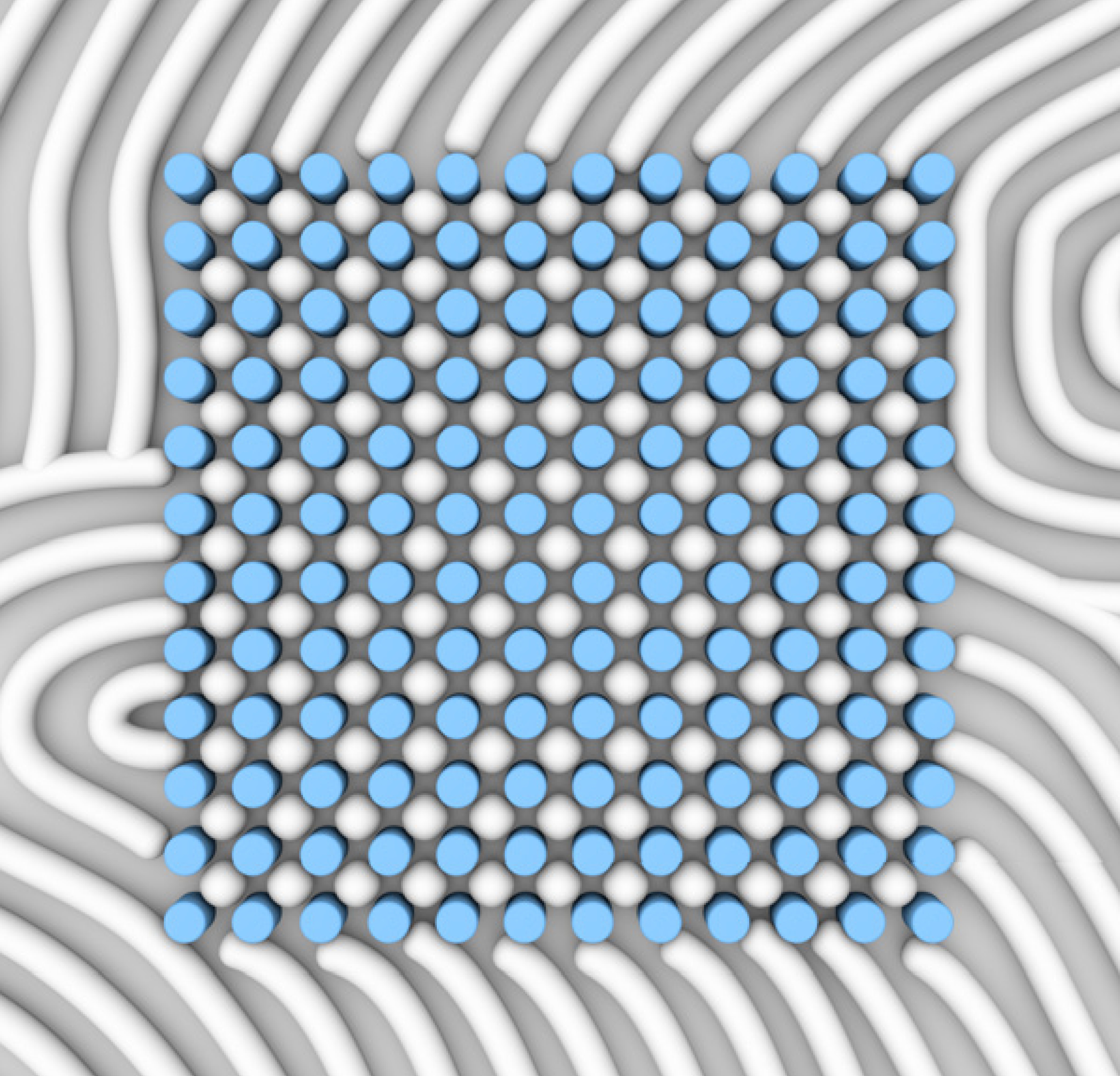
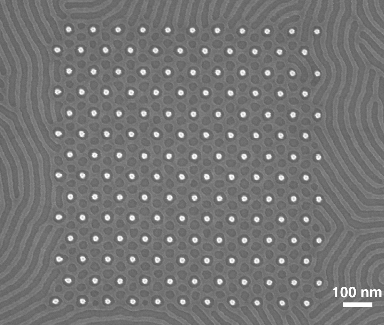
In the new paper, the researchers describe a system for producing arrays of wires that meet at right angles, forming squares and rectangles. While these shapes are the basis for most microchip circuit layouts, they are quite difficult to produce through self-assembly. When molecules self-assemble, explains Caroline Ross, the Toyota Professor of Materials Science and Engineering and a co-author of the papers, they have a natural tendency to create hexagonal shapes — as in a honeycomb or an array of soap bubbles between sheets of glass.
For example, an array of tiny ball bearings in a box “tends to give a hexagonal symmetry, even though it’s in a square box,” Ross says. “But that’s not what circuit designers want. They want patterns with 90-degree angles” — so overcoming that natural tendency was essential to producing a useful self-assembling system, she says.
The team’s solution creates an array of tiny posts on the surface that guides the patterning of the self-assembling polymer molecules. This turns out to have other advantages as well: In addition to producing perfect square and rectangular patterns of tiny polymer wires, the system also enables the creation of a variety of shapes of the material itself, including cylinders, spheres, ellipsoids and double cylinders. “You can generate this astounding array of features,” Ross says, “with a very simple template.”
Karl Berggren, an associate professor of electrical engineering at MIT and a co-author of the paper, explains that these complex shapes are possible because “the template, which is coated so as to repel one of the polymer components, causes a lot of local strain on the pattern. The polymer then twists and turns to try to avoid this strain, and in so doing rearranges on the surface. So we can defeat the polymer’s natural inclinations, and make it create much more interesting patterns.”
This system can also produce features, such as arrays of holes in the material, whose spacing is much closer than what can be achieved using conventional chip-making methods. That means it can produce much more closely packed features on the chip than today’s methods can create — an important step in the ongoing efforts to pack more and more electronic components onto a given microchip.
“This new technique can produce multiple [shapes or patterns] simultaneously,” Tavakkoli says. It can also make “complex patterns, which is an objective for nanodevice fabrication,” with fewer steps than current processes. Fabricating a large area of complex circuitry on a chip using electron-beam lithography “could take several months,” he says. By contrast, using the self-assembling polymer method would take only a few days.
That’s still far too long for manufacturing a commercial product, but Ross explains that this step needs to be done only once to create a master pattern, which can then be used to stamp a coating on other chips in a very rapid fabrication process.
The technique could extend beyond microchip fabrication as well, Ross says. For example, one approach to the quest to pack ever-greater amounts of data onto magnetic media such as computer hard disks is to use a magnetic coating with a very fine pattern stamped into it, precisely defining the areas where each bit of data is to be stored. Such fine patterning could potentially be created using this self-assembly method, she says, and then stamped onto the disks.
Craig Hawker, a professor of chemistry and biochemistry at the University of California at Santa Barbara who was not involved in this work, says, “There is a growing need and requirement for industry to find an alternative to traditional photolithography for the fabrication of cutting-edge microelectronic devices. This work represents a pivotal achievement in this area and clearly demonstrates that structures once considered impossible to achieve by a self-assembly strategy can now be prepared with a high degree of fidelity."
Tavakkoli and Ross’ colleagues in this work are DMSE doctoral students Adam Hannon and Kevin Gotrik, DMSE professor Alfredo Alexander-Katz and EECS professor Karl Berggren. The research, which included work at MIT’s Nanostructures Laboratory and Scanning-Electron-Beam Lithography facility, was funded by the Semiconductor Research Corporation, the Center on Functional Engineered Nano Architectonics, the National Resources Institute, the Singapore-MIT Alliance, the National Science Foundation, the Taiwan Semiconductor Manufacturing Company and Tokyo Electron.
The new method — developed by MIT visiting doctoral student Amir Tavakkoli of the National University of Singapore, along with two other graduate students and three professors in MIT’s departments of Electrical Engineering and Computer Science (EECS) and Materials Science and Engineering (DMSE) — is described in a paper to be published this August in the journal Advanced Materials; the paper is available online now.
The process is closely related to a method the same team described last month in a paper in Science, which makes it possible to produce three-dimensional configurations of wires and connections using a similar system of self-assembling polymers.
In the new paper, the researchers describe a system for producing arrays of wires that meet at right angles, forming squares and rectangles. While these shapes are the basis for most microchip circuit layouts, they are quite difficult to produce through self-assembly. When molecules self-assemble, explains Caroline Ross, the Toyota Professor of Materials Science and Engineering and a co-author of the papers, they have a natural tendency to create hexagonal shapes — as in a honeycomb or an array of soap bubbles between sheets of glass.
For example, an array of tiny ball bearings in a box “tends to give a hexagonal symmetry, even though it’s in a square box,” Ross says. “But that’s not what circuit designers want. They want patterns with 90-degree angles” — so overcoming that natural tendency was essential to producing a useful self-assembling system, she says.
The team’s solution creates an array of tiny posts on the surface that guides the patterning of the self-assembling polymer molecules. This turns out to have other advantages as well: In addition to producing perfect square and rectangular patterns of tiny polymer wires, the system also enables the creation of a variety of shapes of the material itself, including cylinders, spheres, ellipsoids and double cylinders. “You can generate this astounding array of features,” Ross says, “with a very simple template.”
Karl Berggren, an associate professor of electrical engineering at MIT and a co-author of the paper, explains that these complex shapes are possible because “the template, which is coated so as to repel one of the polymer components, causes a lot of local strain on the pattern. The polymer then twists and turns to try to avoid this strain, and in so doing rearranges on the surface. So we can defeat the polymer’s natural inclinations, and make it create much more interesting patterns.”
This system can also produce features, such as arrays of holes in the material, whose spacing is much closer than what can be achieved using conventional chip-making methods. That means it can produce much more closely packed features on the chip than today’s methods can create — an important step in the ongoing efforts to pack more and more electronic components onto a given microchip.
“This new technique can produce multiple [shapes or patterns] simultaneously,” Tavakkoli says. It can also make “complex patterns, which is an objective for nanodevice fabrication,” with fewer steps than current processes. Fabricating a large area of complex circuitry on a chip using electron-beam lithography “could take several months,” he says. By contrast, using the self-assembling polymer method would take only a few days.
That’s still far too long for manufacturing a commercial product, but Ross explains that this step needs to be done only once to create a master pattern, which can then be used to stamp a coating on other chips in a very rapid fabrication process.
The technique could extend beyond microchip fabrication as well, Ross says. For example, one approach to the quest to pack ever-greater amounts of data onto magnetic media such as computer hard disks is to use a magnetic coating with a very fine pattern stamped into it, precisely defining the areas where each bit of data is to be stored. Such fine patterning could potentially be created using this self-assembly method, she says, and then stamped onto the disks.
Craig Hawker, a professor of chemistry and biochemistry at the University of California at Santa Barbara who was not involved in this work, says, “There is a growing need and requirement for industry to find an alternative to traditional photolithography for the fabrication of cutting-edge microelectronic devices. This work represents a pivotal achievement in this area and clearly demonstrates that structures once considered impossible to achieve by a self-assembly strategy can now be prepared with a high degree of fidelity."
Tavakkoli and Ross’ colleagues in this work are DMSE doctoral students Adam Hannon and Kevin Gotrik, DMSE professor Alfredo Alexander-Katz and EECS professor Karl Berggren. The research, which included work at MIT’s Nanostructures Laboratory and Scanning-Electron-Beam Lithography facility, was funded by the Semiconductor Research Corporation, the Center on Functional Engineered Nano Architectonics, the National Resources Institute, the Singapore-MIT Alliance, the National Science Foundation, the Taiwan Semiconductor Manufacturing Company and Tokyo Electron.