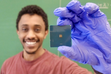
The vast majority of computing devices today are made from silicon, the second most abundant element on Earth, after oxygen. Silicon can be found in various forms in rocks, clay, sand, and soil. And while it is not the best semiconducting material that exists on the planet, it is by far the most readily available. As such, silicon is the dominant material used in most electronic devices, including sensors, solar cells, and the integrated circuits within our computers and smartphones.
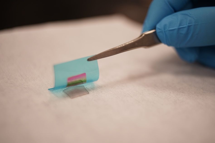
Now MIT engineers have developed a technique to fabricate ultrathin semiconducting films made from a host of exotic materials other than silicon. To demonstrate their technique, the researchers fabricated flexible films made from gallium arsenide, gallium nitride, and lithium fluoride — materials that exhibit better performance than silicon but until now have been prohibitively expensive to produce in functional devices.
The new technique, researchers say, provides a cost-effective method to fabricate flexible electronics made from any combination of semiconducting elements, that could perform better than current silicon-based devices.
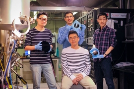
“We’ve opened up a way to make flexible electronics with so many different material systems, other than silicon,” says Jeehwan Kim, the Class of 1947 Career Development Associate Professor in the departments of Mechanical Engineering and Materials Science and Engineering. Kim envisions the technique can be used to manufacture low-cost, high-performance devices such as flexible solar cells, and wearable computers and sensors.
Details of the new technique are reported today in Nature Materials. In addition to Kim, the paper’s MIT co-authors include Wei Kong, Huashan Li, Kuan Qiao, Yunjo Kim, Kyusang Lee, Doyoon Lee, Tom Osadchy, Richard Molnar, Yang Yu, Sang-hoon Bae, Yang Shao-Horn, and Jeffrey Grossman, along with researchers from Sun Yat-Sen University, the University of Virginia, the University of Texas at Dallas, the U.S. Naval Research Laboratory, Ohio State University, and Georgia Tech.
Now you see it, now you don’t
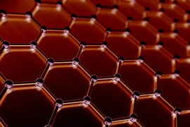
In 2017, Kim and his colleagues devised a method to produce “copies” of expensive semiconducting materials using graphene — an atomically thin sheet of carbon atoms arranged in a hexagonal, chicken-wire pattern. They found that when they stacked graphene on top of a pure, expensive wafer of semiconducting material such as gallium arsenide, then flowed atoms of gallium and arsenide over the stack, the atoms appeared to interact in some way with the underlying atomic layer, as if the intermediate graphene were invisible or transparent. As a result, the atoms assembled into the precise, single-crystalline pattern of the underlying semiconducting wafer, forming an exact copy that could then easily be peeled away from the graphene layer.
The technique, which they call “remote epitaxy,” provided an affordable way to fabricate multiple films of gallium arsenide, using just one expensive underlying wafer.
Soon after they reported their first results, the team wondered whether their technique could be used to copy other semiconducting materials. They tried applying remote epitaxy to silicon, and also germanium — two inexpensive semiconductors — but found that when they flowed these atoms over graphene they failed to interact with their respective underlying layers. It was as if graphene, previously transparent, became suddenly opaque, preventing atoms of silicon and germanium from “seeing” the atoms on the other side.
As it happens, silicon and germanium are two elements that exist within the same group of the periodic table of elements. Specifically, the two elements belong in group four, a class of materials that are ionically neutral, meaning they have no polarity.
“This gave us a hint,” says Kim.
Perhaps, the team reasoned, atoms can only interact with each other through graphene if they have some ionic charge. For instance, in the case of gallium arsenide, gallium has a negative charge at the interface, compared with arsenic’s positive charge. This charge difference, or polarity, may have helped the atoms to interact through graphene as if it were transparent, and to copy the underlying atomic pattern.
“We found that the interaction through graphene is determined by the polarity of the atoms. For the strongest ionically bonded materials, they interact even through three layers of graphene,” Kim says. “It’s similar to the way two magnets can attract, even through a thin sheet of paper.”
Opposites attract
The researchers tested their hypothesis by using remote epitaxy to copy semiconducting materials with various degrees of polarity, from neutral silicon and germanium, to slightly polarized gallium arsenide, and finally, highly polarized lithium fluoride — a better, more expensive semiconductor than silicon.
They found that the greater the degree of polarity, the stronger the atomic interaction, even, in some cases, through multiple sheets of graphene. Each film they were able to produce was flexible and merely tens to hundreds of nanometers thick.
The material through which the atoms interact also matters, the team found. In addition to graphene, they experimented with an intermediate layer of hexagonal boron nitride (hBN), a material that resembles graphene’s atomic pattern and has a similar Teflon-like quality, enabling overlying materials to easily peel off once they are copied.
However, hBN is made of oppositely charged boron and nitrogen atoms, which generate a polarity within the material itself. In their experiments, the researchers found that any atoms flowing over hBN, even if they were highly polarized themselves, were unable to interact with their underlying wafers completely, suggesting that the polarity of both the atoms of interest and the intermediate material determines whether the atoms will interact and form a copy of the original semiconducting wafer.
“Now we really understand there are rules of atomic interaction through graphene,” Kim says.
With this new understanding, he says, researchers can now simply look at the periodic table and pick two elements of opposite charge. Once they acquire or fabricate a main wafer made from the same elements, they can then apply the team’s remote epitaxy techniques to fabricate multiple, exact copies of the original wafer.
“People have mostly used silicon wafers because they’re cheap,” Kim says.
“Now our method opens up a way to use higher-performing, nonsilicon materials. You can just purchase one expensive wafer and copy it over and over again, and keep reusing the wafer. And now the material library for this technique is totally expanded.”
Kim envisions that remote epitaxy can now be used to fabricate ultrathin, flexible films from a wide variety of previously exotic, semiconducting materials — as long as the materials are made from atoms with a degree of polarity. Such ultrathin films could potentially be stacked, one on top of the other, to produce tiny, flexible, multifunctional devices, such as wearable sensors, flexible solar cells, and even, in the distant future, “cellphones that attach to your skin.”
“In smart cities, where we might want to put small computers everywhere, we would need low power, highly sensitive computing and sensing devices, made from better materials,” Kim says. “This [study] unlocks the pathway to those devices.”
This research was supported in part by the Defense Advanced Research Projects Agency, the Department of Energy, the Air Force Research Laboratory, LG Electronics, Amore Pacific, LAM Research, and Analog Devices.
