MIT scientists and their colleagues have created a simple superconducting device that could transfer current through electronic devices much more efficiently than is possible today. As a result, the new diode, a kind of switch, could dramatically cut the amount of energy used in high-power computing systems, a major problem that is estimated to become much worse. Even though it is in the early stages of development, the diode is more than twice as efficient as similar ones reported by others. It could even be integral to emerging quantum computing technologies.
The work, which is reported in the July 13 online issue of Physical Review Letters, is also the subject of a news story in Physics Magazine.
“This paper showcases that the superconducting diode is an entirely solved problem from an engineering perspective,” says Philip Moll, director of the Max Planck Institute for the Structure and Dynamics of Matter in Germany. Moll was not involved in the work. “The beauty of [this] work is that [Moodera and colleagues] obtained record efficiencies without even trying [and] their structures are far from optimized yet.”
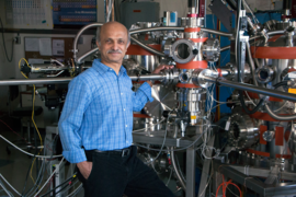
“Our engineering of a superconducting diode effect that is robust and can operate over a wide temperature range in simple systems can potentially open the door for novel technologies,” says Jagadeesh Moodera, leader of the current work and a senior research scientist in MIT’s Department of Physics. Moodera is also affiliated with the Materials Research Laboratory, the Francis Bitter Magnet Laboratory, and the Plasma Science and Fusion Center (PSFC).
The nanoscopic rectangular diode — about 1,000 times thinner than the diameter of a human hair — is easily scalable. Millions could be produced on a single silicon wafer.
Toward a superconducting switch
Diodes, devices that allow current to travel easily in one direction but not in the reverse, are ubiquitous in computing systems. Modern semiconductor computer chips contain billions of diode-like devices known as transistors. However, these devices can get very hot due to electrical resistance, requiring vast amounts of energy to cool the high-power systems in the data centers behind myriad modern technologies, including cloud computing. According to a 2018 news feature in Nature, these systems could use nearly 20 percent of the world’s power in 10 years.
As a result, work toward creating diodes made of superconductors has been a hot topic in condensed matter physics. That’s because superconductors transmit current with no resistance at all below a certain low temperature (the critical temperature), and are therefore much more efficient than their semiconducting cousins, which have noticeable energy loss in the form of heat.
Until now, however, other approaches to the problem have involved much more complicated physics. “The effect we found is due [in part] to a ubiquitous property of superconductors that can be realized in a very simple, straightforward manner. It just stares you in the face,” says Moodera.
Says Moll of the Max Planck Institute, “The work is an important counterpoint to the current fashion to associate superconducting diodes [with] exotic physics, such as finite-momentum pairing states. While in reality, a superconducting diode is a common and widespread phenomenon present in classical materials, as a result of certain broken symmetries.”
A somewhat serendipitous discovery
In 2020 Moodera and colleagues observed evidence of an exotic particle pair known as Majorana fermions. These particle pairs could lead to a new family of topological qubits, the building blocks of quantum computers. While pondering approaches to creating superconducting diodes, the team realized that the material platform they developed for the Majorana work might also be applied to the diode problem.
They were right. Using that general platform, they developed different iterations of superconducting diodes, each more efficient than the last. The first, for example, consisted of a nanoscopically thin layer of vanadium, a superconductor, which was patterned into a structure common to electronics (the Hall bar). When they applied a tiny magnetic field comparable to the Earth’s magnetic field, they saw the diode effect — a giant polarity dependence for current flow.
They then created another diode, this time layering a superconductor with a ferromagnet (a ferromagnetic insulator in their case), a material that produces its own tiny magnetic field. After applying a tiny magnetic field to magnetize the ferromagnet so that it produces its own field, they found an even bigger diode effect that was stable even after the original magnetic field was turned off.
Ubiquitous properties
The team went on to figure out what was happening.
In addition to transmitting current with no resistance, superconductors also have other, less well-known but just as ubiquitous properties. For example, they don’t like magnetic fields getting inside. When exposed to a tiny magnetic field, superconductors produce an internal supercurrent that induces its own magnetic flux that cancels the external field, thereby maintaining their superconducting state. This phenomenon, known as the Meissner screening effect, can be thought of as akin to our bodies’ immune system releasing antibodies to fight the infection of bacteria and other pathogens. This works, however, only up to some limit. Similarly, superconductors cannot entirely keep out large magnetic fields.
The diodes the team created make use of this universal Meissner screening effect. The tiny magnetic field they applied — either directly, or through the adjacent ferromagnetic layer — activates the material’s screening current mechanism for expelling the external magnetic field and maintaining superconductivity.
The team also found that another key factor in optimizing these superconductor diodes is tiny differences between the two sides, or edges, of the diode devices. These differences “create some sort of asymmetry in the way the magnetic field enters the superconductor,” Moodera says.
By engineering their own form of edges on diodes to optimize these differences — for example, one edge with sawtooth features, while the other edge not intentionally altered — the team found that they could increase the efficiency from 20 percent to more than 50 percent. This discovery opens the door for devices whose edges could be “tuned” for even higher efficiencies, Moodera says.
In sum, the team discovered that the edge asymmetries within superconducting diodes, the ubiquitous Meissner screening effect found in all superconductors, and a third property of superconductors known as vortex pinning all came together to produce the diode effect.
“It is fascinating to see how inconspicuous yet ubiquitous factors can create a significant effect in observing the diode effect,” says Yasen Hou, first author of the paper and a postdoc at the Francis Bitter Magnet Laboratory and the PSFC. “What’s more exciting is that [this work] provides a straightforward approach with huge potential to further improve the efficiency.”
Christoph Strunk is a professor at the University of Regensburg in Germany. Says Strunk, who was not involved in the research, “the present work demonstrates that the supercurrent in simple superconducting strips can become nonreciprocal. Moreover, when combined with a ferromagnetic insulator, the diode effect can even be maintained in the absence of an external magnetic field. The rectification direction can be programmed by the remnant magnetization of the magnetic layer, which may have high potential for future applications. The work is important and appealing both from the basic research and from the applications point of view.”
Teenage contributors
Moodera noted that the two researchers who created the engineered edges did so while still in high school during a summer at Moodera’s lab. They are Ourania Glezakou-Elbert of Richland, Washington, who will be going to Princeton University this fall, and Amith Varambally of Vestavia Hills, Alabama, who will be entering Caltech.
Says Varambally, “I didn't know what to expect when I set foot in Boston last summer, and certainly never expected to [be] a coauthor in a Physical Review Letters paper.
“Every day was exciting, whether I was reading dozens of papers to better understand the diode phenomena, or operating machinery to fabricate new diodes for study, or engaging in conversations with Ourania, Dr. Hou, and Dr. Moodera about our research.
“I am profoundly grateful to Dr. Moodera and Dr. Hou for providing me with the opportunity to work on such a fascinating project, and to Ourania for being a great research partner and friend.”
In addition to Moodera and Hou, corresponding authors of the paper are professors Patrick A. Lee of the MIT Department of Physics and Akashdeep Kamra of Autonomous University of Madrid. Other authors from MIT are Liang Fu and Margarita Davydova of the Department of Physics, and Hang Chi, Alessandro Lodesani, and Yingying Wu, all of the Francis Bitter Magnet Laboratory and the Plasma Science and Fusion Center. Chi is also affiliated with the U.S. Army CCDC Research Laboratory.
Authors also include Fabrizio Nichele, Markus F. Ritter, and Daniel Z. Haxwell of IBM Research Europe; Stefan Ilić of Materials Physics Center (CFM-MPC); and F. Sebastian Bergeret of CFM-MPC and Donostia International Physics Center.
This work was supported by the Air Force Office of Sponsored Research, the Office of Naval Research, the National Science Foundation, and the Army Research Office. Additional funders are the European Research Council, the European Union’s Horizon 2020 Research and Innovation Framework Programme, the Spanish Ministry of Science and Innovation, the A. v. Humboldt Foundation, and the Department of Energy’s Office of Basic Sciences.