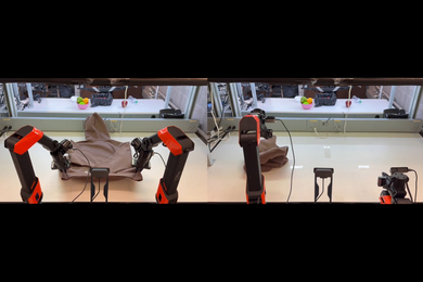

MIT researchers have developed a novel cryptography circuit that can be used to protect low-power “internet of things” (IoT) devices in the coming age of quantum computing.
Quantum computers can in principle execute calculations that today are practically impossible for classical computers. Bringing quantum computers online and to market could one day enable advances in medical research, drug discovery, and other applications. But there’s a catch: If hackers also have access to quantum computers, they could potentially break through the powerful encryption schemes that currently protect data exchanged between devices.
Today’s most promising quantum-resistant encryption scheme is called “lattice-based cryptography,” which hides information in extremely complicated mathematical structures. To date, no known quantum algorithm can break through its defenses. But these schemes are way too computationally intense for IoT devices, which can only spare enough energy for simple data processing.
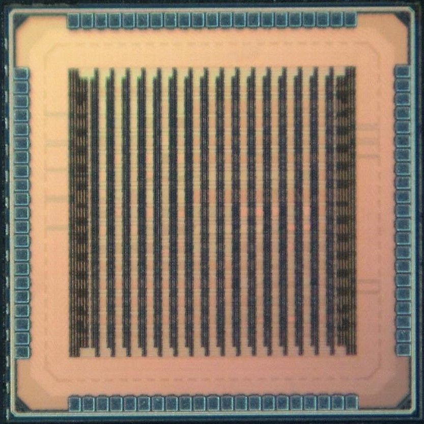
In a paper presented at the recent International Solid-State Circuits Conference, MIT researchers describe a novel circuit architecture and statistical optimization tricks that can be used to efficiently compute lattice-based cryptography. The 2-millimeter-squared chips the team developed are efficient enough for integration into any current IoT device.
The architecture is customizable to accommodate the multiple lattice-based schemes currently being studied in preparation for the day that quantum computers come online. “That might be a few decades from now, but figuring out if these techniques are really secure takes a long time,” says first author Utsav Banerjee, a graduate student in electrical engineering and computer science. “It may seem early, but earlier is always better.”
Moreover, the researchers say, the circuit is the first of its kind to meet standards for lattice-based cryptography set by the National Institute of Standards and Technology (NIST), an agency of the U.S. Department of Commerce that finds and writes regulations for today’s encryption schemes.
Joining Banerjee on the paper are Anantha Chandrakasan, dean of MIT’s School of Engineering and the Vannevar Bush Professor of Electrical Engineering and Computer Science, and Abhishek Pathak of the Indian Institute of Technology.
Efficient sampling
In the mid-1990s, MIT Professor Peter Shor developed a quantum algorithm that can essentially break through all modern cryptography schemes. Since then, NIST has been trying to find the most secure postquantum encryption schemes. This happens in phases; each phase winnows down a list of the most secure and practical schemes. Two weeks ago, the agency entered its second phase for postquantum cryptography, with lattice-based schemes making up half of its list.
In the new study, the researchers first implemented on commercial microprocessors several NIST lattice-based cryptography schemes from the agency’s first phase. This revealed two bottlenecks for efficiency and performance: generating random numbers and data storage.
Generating random numbers is the most important part of all cryptography schemes, because those numbers are used to generate secure encryption keys that can’t be predicted. That’s calculated through a two-part process called “sampling.”
Sampling first generates pseudorandom numbers from a known, finite set of values that have an equal probability of being selected. Then, a “postprocessing” step converts those pseudorandom numbers into a different probability distribution with a specified standard deviation — a limit for how much the values can vary from one another — that randomizes the numbers further. Basically, the random numbers must satisfy carefully chosen statistical parameters. This difficult mathematical problem consumes about 80 percent of all computation energy needed for lattice-based cryptography.
After analyzing all available methods for sampling, the researchers found that one method, called SHA-3, can generate many pseudorandom numbers two or three times more efficiently than all others. They tweaked SHA-3 to handle lattice-based cryptography sampling. On top of this, they applied some mathematical tricks to make pseudorandom sampling, and the postprocessing conversion to new distributions, faster and more efficient.
They run this technique using energy-efficient custom hardware that takes up only 9 percent of the surface area of their chip. In the end, this makes the process of sampling two orders of magnitude more efficient than traditional methods.
Splitting the data
On the hardware side, the researchers made innovations in data flow. Lattice-based cryptography processes data in vectors, which are tables of a few hundred or thousand numbers. Storing and moving those data requires physical memory components that take up around 80 percent of the hardware area of a circuit.
Traditionally, the data are stored on a single two-or four-port random access memory (RAM) device. Multiport devices enable the high data throughput required for encryption schemes, but they take up a lot of space.
For their circuit design, the researchers modified a technique called “number theoretic transform” (NTT), which functions similarly to the Fourier transform mathematical technique that decomposes a signal into the multiple frequencies that make it up. The modified NTT splits vector data and allocates portions across four single-port RAM devices. Each vector can still be accessed in its entirety for sampling as if it were stored on a single multiport device. The benefit is the four single-port REM devices occupy about a third less total area than one multiport device.
“We basically modified how the vector is physically mapped in the memory and modified the data flow, so this new mapping can be incorporated into the sampling process. Using these architecture tricks, we reduced the energy consumption and occupied area, while maintaining the desired throughput,” Banerjee says.
The circuit also incorporates a small instruction memory component that can be programmed with custom instructions to handle different sampling techniques — such as specific probability distributions and standard deviations — and different vector sizes and operations. This is especially helpful, as lattice-based cryptography schemes will most likely change slightly in the coming years and decades.
Adjustable parameters can also be used to optimize efficiency and security. The more complex the computation, the lower the efficiency, and vice versa. In their paper, the researchers detail how to navigate these tradeoffs with their adjustable parameters. Next, the researchers plan to tweak the chip to run all the lattice-based cryptography schemes listed in NIST’s second phase.
The work was supported by Texas Instruments and the TSMC University Shuttle Program.