
If you were to pry open your smartphone, you would see an array of electronic chips and components laid out across a circuit board, like a miniature city. Each component might contain even smaller “chiplets,” some no wider than a human hair. These elements are often assembled with robotic grippers designed to pick up the components and place them down in precise configurations.
As circuit boards are packed with ever smaller components, however, robotic grippers’ ability to manipulate these objects is approaching a limit.
“Electronics manufacturing requires handling and assembling small components in a size similar to or smaller than grains of flour,” says Sanha Kim, a former MIT postdoc and research scientist who worked in the lab of mechanical engineering associate professor John Hart. “So a special pick-and-place solution is needed, rather than simply miniaturizing [existing] robotic grippers and vacuum systems.”
Now Kim, Hart, and others have developed a miniature “electroadhesive” stamp that can pick up and place down objects as small as 20 nanometers wide — about 1,000 times finer than a human hair. The stamp is made from a sparse forest of ceramic-coated carbon nanotubes arranged like bristles on a tiny brush.
When a small voltage is applied to the stamp, the carbon nanotubes become temporarily charged, forming prickles of electrical attraction that can attract a minute particle. By turning the voltage off, the stamp’s “stickiness” goes away, enabling it to release the object onto a desired location.
Hart says the stamping technique can be scaled up to a manufacturing setting to print micro- and nanoscale features, for instance to pack more elements onto ever smaller computer chips. The technique may also be used to pattern other small, intricate features, such as cells for artificial tissues. And, the team envisions macroscale, bioinspired electroadhesive surfaces, such as voltage-activated pads for grasping everyday objects and for gecko-like climbing robots.
“Simply by controlling voltage, you can switch the surface from basically having zero adhesion to pulling on something so strongly, on a per unit area basis, that it can act somewhat like a gecko’s foot,” Hart says.
The team has published its results today in the journal Science Advances.
The team also includes Michael Boutilier, a former postdoc at MIT and now Assistant Professor at Western University in Ontario, MIT Ph.D. student Nigamaa Nayakanti, MIT postdoc Changhong Cao, and collaborators from the University of Pennsylvania including Prof. Kevin Turner.
Like dry Scotch tape
Existing mechanical grippers are unable to pick up objects smaller than about 50 to 100 microns, mainly because at smaller scales surface forces tend to win over gravity. You may see this when pouring flour from a spoon — inevitably, some tiny particles stick to the spoon’s surface, rather than letting gravity drag them off.
“The dominance of surface forces over gravity forces becomes a problem when trying to precisely place smaller things — which is the foundational process by which electronics are assembled into integrated systems,” Hart says.
He and his colleagues noted that electroadhesion, the process of adhering materials via an applied voltage, has been used in some industrial settings to pick and place large objects, such as fabrics, textiles, and whole silicon wafers. But this same electroadhesion had never been applied to objects at the microscopic level, because a new material design for controlling electroadhesion at smaller scales was needed.
Hart’s group has previously worked with carbon nanotubes (CNTs) — atoms of carbon linked in a lattice pattern and rolled into microscopic tubes. CNTs are known for their exceptional mechanical, electrical, and chemical properties, and they have been widely studied as dry adhesives.
“Previous work on CNT-based dry adhesives focused on maximizing the contact area of the nanotubes to essentially create a dry Scotch tape,” Hart says. “We took the opposite approach, and said, ‘let’s design a nanotube surface to minimize the contact area, but use electrostatics to turn on adhesion when we need it.’”
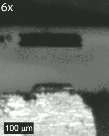
New electroadhesive stamp picks and places a 170-micrometer sized LED chiplet, using an external voltage of 30V to temporarily “stick” to the LED. Courtesy of the researchers
A sticky on/off switch
The team found that if they coated CNTs with a thin dielectric material such as aluminum oxide, when they applied a voltage to the nanotubes, the ceramic layer became polarized, meaning its positive and negative charges became temporarily separated. For instance, the positive charges of the tips of the nanotubes induced an opposite polarization in any nearby conducting material, such as a microscopic electronic element.
As a result, the nanotube-based stamp adhered to the element, picking it up like tiny, electrostatic fingers. When the researchers turned the voltage off, the nanotubes and the element depolarized, and the “stickiness” went away, allowing the stamp to detach and place the object onto a given surface.
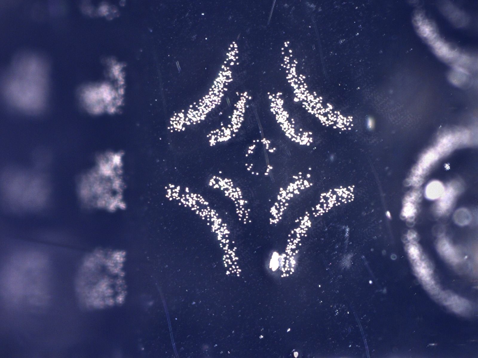
The team explored various formulations of stamp designs, altering the density of carbon nanotubes grown on the stamp, as well as the thickness of the ceramic layer that they used to coat each nanotube. They found that the thinner the ceramic layer and the more sparsely spaced the carbon nanotubes were, the greater the stamp’s on/off ratio, meaning the greater the stamp’s stickiness was when the voltage was on, versus when it was off.
In their experiments, the team used the stamp to pick up and place down films of nanowires, each about 1,000 times thinner than a human hair. They also used the technique to pick and place intricate patterns of polymer and metal microparticles, as well as micro-LEDs.
Hart says the electroadhesive printing technology could be scaled up to manufacture circuit boards and systems of miniature electronic chips, as well as displays with microscale LED pixels.
“With ever-advancing capabilities of semiconductor devices, an important need and opportunity is to integrate smaller and more diverse components, such as microprocessors, sensors, and optical devices,” Hart says. “Often, these are necessarily made separately but must be integrated together to create next-generation electronic systems. Our technology possibly bridges the gap necessary for scalable, cost-effective assembly of these systems.”
This research was supported in part by the Toyota Research Insititute, the National Science Foundation, and the MIT-Skoltech Next Generation Program.