Researchers at Lincoln Laboratory have been using silicon and compound semiconductor substrates to build photonic integrated circuits, or PICs, that enable devices such as optical communication receivers, wideband ladar transmitters, interconnects for trapped-ion quantum computers, inertial sensors, and microwave signal processors. Now, a recently awarded state grant will fund a germanium deposition reactor that will allow the researchers to exploit germanium as a key optoelectronic material in the fabrication of PICs operating at nontraditional wavelengths and under harsh environmental conditions.
Photonic integrated circuits are in demand for routing the enormous volume of traffic passing through data centers today. In addition, high-speed, reliable photonic circuits that lessen systems' electrical power requirements can improve the performance of quantum and all-optical computing systems, as well as the throughput of the advanced microprocessors embedded in highly sensitive sensors and increasingly capable autonomous vehicles.
"The addition of the reactor will allow Lincoln Laboratory to manufacture trusted silicon photonic integrated circuits," says Daniel Pulver, the manager of Lincoln Laboratory's Microelectronics Laboratory.
The semiconductor facility has already been certified as a Trusted Foundry by the Defense Microelectronics Activity Trusted Program, which was established by the Department of Defense (DoD) and the National Security Agency to assure the security of the fabrication process and supply chain behind microelectronics used in defense systems. Pulver said that this grant will enable Lincoln Laboratory's microelectronics facility to become the first DoD trusted silicon photonics foundry.
The improved in-house capabilities that the reactor will bring to the Microelectronics Laboratory will also support innovations that Lincoln Laboratory is developing, for example, low-size, low-weight, and low-power inertial navigation sensors. Currently, the laboratory has to outsource the deposition of germanium on silicon PICs that require such deposition for some of the systems under development. The new germanium reactor will allow this deposition to be performed in-house to facilitate reduced fabrication time for next-generation photonic integrated circuits.
"This tool will allow us to optimize germanium-based photodetectors for operation at cryogenic temperatures, develop new classes of optical modulators, and extend the operating wavelength range of photonic integrated circuits to the long-wavelength infrared region of the spectrum," says Paul Juodawlkis, assistant leader of the Quantum Information and Integrated Nanosystems Group and principal investigator for Lincoln Laboratory's integrated photonics activities.
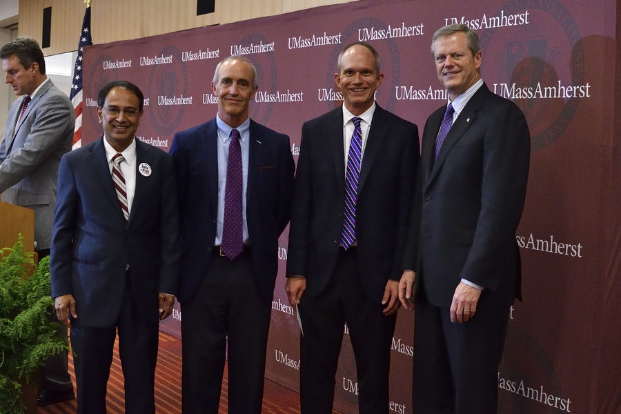
Massachusetts Governor Charlie Baker and Secretary of Housing and Economic Development Jay Ash presented the $1.9 million grant award to Lincoln Laboratory to celebrate National Manufacturing Day earlier this fall. It was one of seven grants awarded this year under the Massachusetts Manufacturing Innovation Initiative (M2I2) to support infrastructure improvements that will enable research and development leading to the manufacturing of advanced functional fabrics, integrated photonics, robotics, and flexible hybrid electronics.
"These awards will ensure the Commonwealth remains a leader in advanced manufacturing to spur job growth and train students for valuable career opportunities," Baker said.
The M2I2 was established to facilitate Massachusetts' participation in the Manufacturing USA program, a network of regional institutes, each with a distinct technology focus, whose member organizations collaborate to leverage existing resources, to foster education, and to promote manufacturing innovation and commercialization. Currently, nine institutes with main offices in cities across the country are connecting member organizations from academia, industry, and the research community.
Lincoln Laboratory has also become a member of AIM Photonics (American Institute for Manufacturing Integrated Photonics), a Manufacturing USA institute headquartered in Rochester, New York. The M2I2 grant will accelerate Lincoln Laboratory's involvement with AIM Photonics through advanced process development, internship and apprenticeship opportunities, and engagement with companies in Massachusetts and throughout the nation.
"We look forward to partnering with AIM Photonics and the Commonwealth on these exciting activities," Juodawlkis says. "We plan to use these new resources as a springboard to provide educational outreach and internships to students at both universities and community colleges."
