
A new technique developed by MIT researchers reveals the inner details of photonic crystals, synthetic materials whose exotic optical properties are the subject of widespread research.
Photonic crystals are generally made by drilling millions of closely spaced, minuscule holes in a slab of transparent material, using variations of microchip-fabrication methods. Depending on the exact orientation, size, and spacing of these holes, these materials can exhibit a variety of peculiar optical properties, including “superlensing,” which allows for magnification that pushes beyond the normal theoretical limits, and “negative refraction,” in which light is bent in a direction opposite to its path through normal transparent materials.
But to understand exactly how light of various colors and from various directions moves through photonic crystals requires extremely complex calculations. Researchers often use highly simplified approaches; for example they may only calculate the behavior of light along a single direction or for a single color.
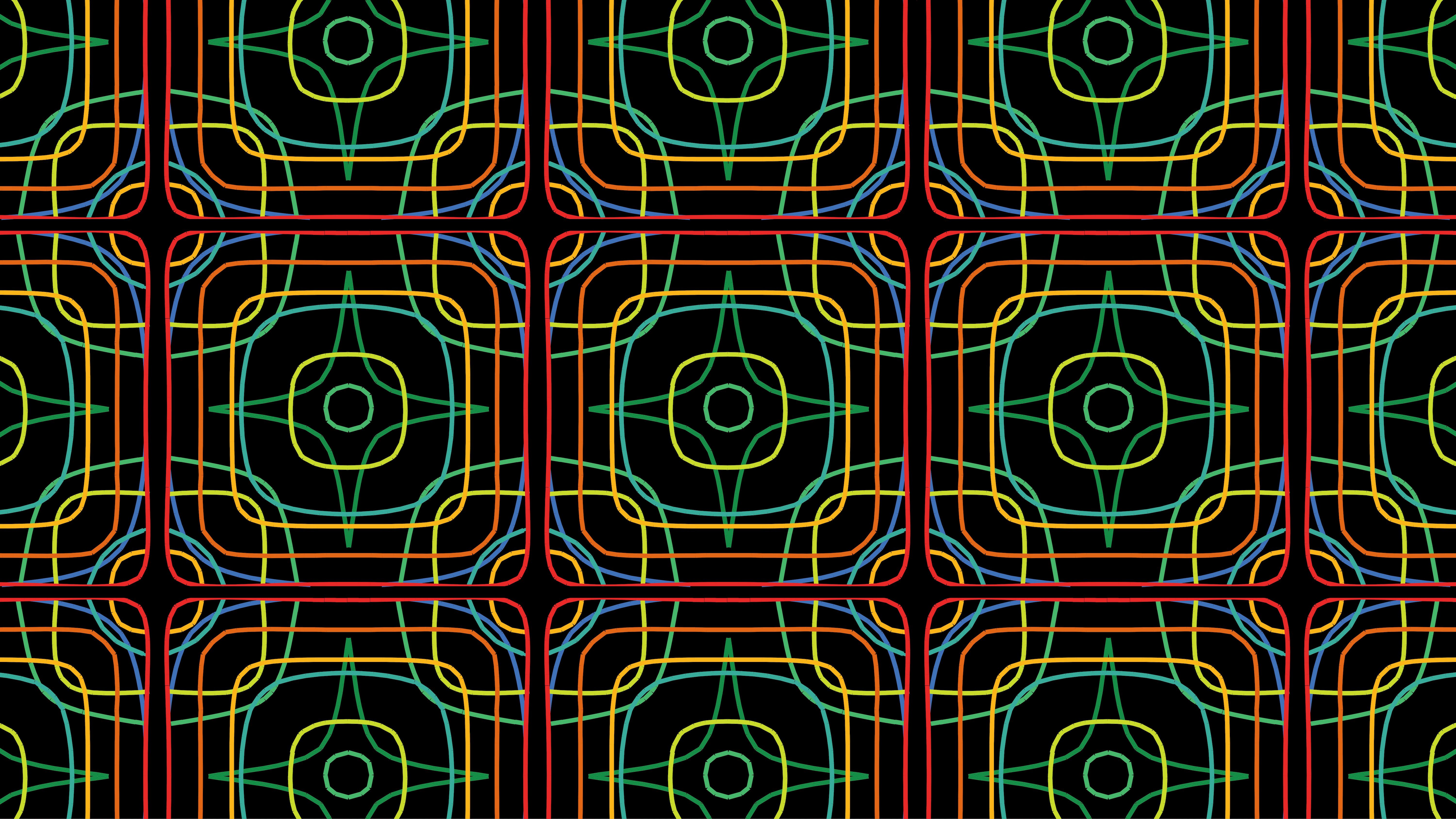
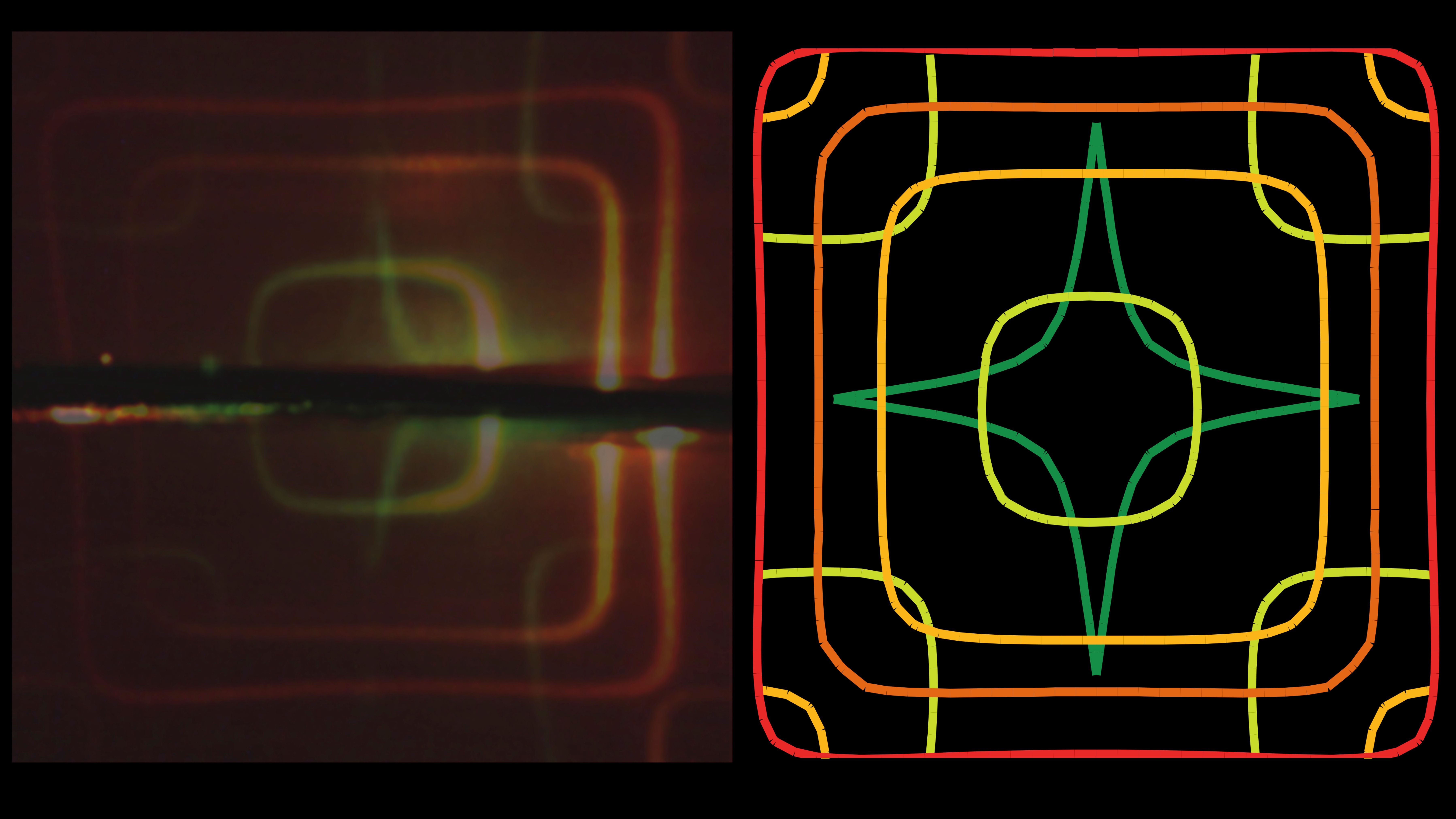
Instead, the new technique makes the full range of information directly visible. Researchers can use a straightforward laboratory setup to display the information — a pattern of so-called “iso-frequency contours” — in a graphical form that can be simply photographed and examined, in many cases eliminating the need for calculations. The method is described this week in the journal Science Advances, in a paper by MIT postdoc Bo Zhen, recent Wellesley College graduate and MIT affiliate Emma Regan, MIT professors of physics Marin Soljačić and John Joannopoulos, and four others.
The discovery of this new technique, Zhen explains, came about by looking closely at a phenomenon that the researchers had noticed and even made use of for years, but whose origins they hadn’t previously understood. Patterns of scattered light seemed to fan out from samples of photonic materials when the samples were illuminated by laser light. The scattering was surprising, since the underlying crystalline structure was fabricated to be almost perfect in these materials.
“When we would try to do a lasing measurement, we would always see this pattern,” Zhen says. “We saw this shape, but we didn’t know what was happening.” But it did help them to get their experimental setup properly aligned, because the scattered light pattern would appear as soon as the laser beam was properly lined up with the crystal. Upon careful analysis, they realized the scattering patterns were generated by tiny defects in the crystal — holes that were not perfectly round in shape or that were slightly tapered from one end to the other.
“There is fabrication disorder even in the best samples that can be made,” Regan says. “People think that the scattering would be very weak, because the sample is nearly perfect,” but it turns out that at certain angles and frequencies, the light scatters very strongly; as much as 50 percent of the incoming light can be scattered. By illuminating the sample in turn with a sequence of different colors, it is possible to build up a full display of the relative paths light beams take, all across the visible spectrum. The scattered light produces a direct view of the iso-frequency contours — a sort of topographic map of the way light beams of different colors bend as they pass through the photonic crystal.
“This is a very beautiful, very direct way to observe the iso-frequency contours,” Soljačić says. “You just shine light at the sample, with the right direction and frequency,” and what comes out is a direct image of the needed information, he says.
The finding could potentially be useful for a number of different applications, the team says. For example, it could lead to a way of making large, transparent display screens, where most light would pass straight through as if through a window, but light of specific frequencies would be scattered to produce a clear image on the screen. Or, the method could be used to make private displays that would only be visible to the person directly in front of the screen.
Because it relies on imperfections in the fabrication of the crystal, this method could also be used as a quality-control measure for manufacturing of such materials; the images provide an indication of not only the total amount of imperfections, but also their specific nature — that is, whether the dominant disorder in the sample comes from noncircular holes or etches that aren’t straight — so that the process can be tuned and improved.
“Using a clever trick, the Soljačić group turned what is ordinarily a nuisance (i.e., unavoidable disorder in nanofabrication) to their advantage,” says Mikael Rechtsman, an assistant professor of physics at Pennsylvania State University who was not involved in this work. “The random scattering caused by the disorder allowed them to directly image the iso-frequency contours of the photonic crystal slab structure. Since any nanofabricated structure always has some degree of disorder, and since disorder is invariably difficult to model a priori in simulations, their method provides an extremely convenient characterization tool for photonic crystal resonant mode band structures.”
Rechtsman adds, “This could become an essential tool in the hunt for high-power single-mode semiconductor lasers (in particular, photonic crystal surface emitting lasers), with wide-ranging applications including telecommunications and manufacturing.”
The team also included researchers at MIT Research Laboratory of Electronics, including Yuichi Igarashi (now at NEC Corporation in Japan), Ido Kaminer, Chia Wei Hsu (now at Yale University), and Yichen Shen. The work was supported by the Army Research Office through the Institute for Soldier Nanotechnologies at MIT, and by the U.S. Department of Energy through S3TEC, an Energy Frontier Center.