Today, computer chips are built by stacking layers of different materials and etching patterns into them.
But in the latest issue of Advanced Materials, MIT researchers and their colleagues report the first chip-fabrication technique that enables significantly different materials to be deposited in the same layer. They also report that, using the technique, they have built chips with working versions of all the circuit components necessary to produce a general-purpose computer.
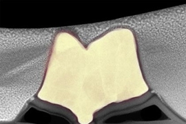
The layers of material in the researchers’ experimental chip are extremely thin — between one and three atoms thick. Consequently, this work could abet efforts to manufacture thin, flexible, transparent computing devices, which could be laminated onto other materials. “The methodology is universal for many kinds of structures,” says Xi Ling, a postdoc in the Research Laboratory of Electronics and one of the paper’s first authors. “This offers us tremendous potential with numerous candidate materials for ultrathin circuit design.”
The technique also has implications for the development of the ultralow-power, high-speed computing devices known as tunneling transistors and, potentially, for the integration of optical components into computer chips.
“It’s a brand new structure, so we should expect some new physics there,” says Yuxuan Lin, a graduate student in electrical engineering and computer science and the paper’s other first author.
Ling and Lin are joined on the paper by Mildred Dresselhaus, an Institute Professor emerita of physics and electrical engineering; Jing Kong, an ITT Career Development Professor of Electrical Engineering; Tomás Palacios, an associate professor of electrical engineering; and by another 10 MIT researchers and two more from Brookhaven National Laboratory and Taiwan’s National Tsing-Hua University.
Strange bedfellows
Computer chips are built from crystalline solids, materials whose atoms are arranged in a regular geometrical pattern known as a crystal lattice. Previously, only materials with closely matched lattices have been deposited laterally in the same layer of a chip. The researchers’ experimental chip, however, uses two materials with very different lattice sizes: molybdenum disulfide and graphene, which is a single-atom-thick layer of carbon.
Moreover, the researchers’ fabrication technique generalizes to any material that, like molybdenum disulfide, combines elements from group six of the periodic table, such as chromium, molybdenum, and tungsten, and elements from group 16, such as sulfur, selenium, and tellurium. Many of these compounds are semiconductors — the type of material that underlies transistor design — and exhibit useful behavior in extremely thin layers.
Graphene, which the researchers chose as their second material, has many remarkable properties. It’s the strongest known material, but it also has the highest known electron mobility, a measure of how rapidly electrons move through it. As such, it’s an excellent candidate for use in thin-film electronics or, indeed, in any nanoscale electronic devices.
To assemble their laterally integrated circuits, the researchers first deposit a layer of graphene on a silicon substrate. Then they etch it away in the regions where they wish to deposit the molybdenum disulfide.
Next, at one end of the substrate, they place a solid bar of a material known as PTAS.
They heat the PTAS and flow a gas across it and across the substrate. The gas carries PTAS molecules with it, and they stick to the exposed silicon but not to the graphene. Wherever the PTAS molecules stick, they catalyze a reaction with another gas that causes a layer of molybdenum disulfide to form.
In previous work, the researchers characterized a range of materials that promote the formation of crystals of other compounds, any of which could be plugged into the process.
Future electronics
The new fabrication method could open the door to more powerful computing if it can be used to produce tunneling-transistor processors. Fundamentally, a transistor is a device that can be modulated to either allow a charge to cross a barrier or prohibit it from crossing. In a tunneling transistor, the charge crosses the barrier by means of a counterintuitive quantum-mechanical effect, in which an electron can be thought of as disappearing at one location and reappearing at another.
These effects are subtle, so they’re more pronounced at extremely small scales, like the one- to three-atom thicknesses of the layers in the researchers’ experimental chip. And, because electron tunneling is immune to the thermal phenomena that limit the efficiency of conventional transistors, tunneling transistors can operate at very low power and could achieve much higher speeds.
"This work is very exciting,” says Philip Kim, a physics professor at Harvard University. “The MIT team demonstrated that controlled stitching of two completely different, atomically thin 2-D materials is possible. The electrical properties of the resulting lateral heterostructures are very impressive."