Chips that use light, rather than electricity, to move data would consume much less power — and energy efficiency is a growing concern as chips’ transistor counts rise.
Of the three chief components of optical circuits — light emitters, modulators, and detectors — emitters are the toughest to build. One promising light source for optical chips is molybdenum disulfide (MoS2), which has excellent optical properties when deposited as a single, atom-thick layer. Other experimental on-chip light emitters have more-complex three-dimensional geometries and use rarer materials, which would make them more difficult and costly to manufacture.
In the next issue of the journal Nano Letters, researchers from MIT’s departments of Physics and of Electrical Engineering and Computer Science will describe a new technique for building MoS2 light emitters tuned to different frequencies, an essential requirement for optoelectronic chips. Since thin films of material can also be patterned onto sheets of plastic, the same work could point toward thin, flexible, bright, color displays.
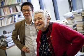
The researchers also provide a theoretical characterization of the physical phenomena that explain the emitters’ tunability, which could aid in the search for even better candidate materials. Molybdenum is one of several elements, clustered together on the periodic table, known as transition metals. “There’s a whole family of transition metals,” says Institute Professor Emeritus Mildred Dresselhaus, the corresponding author on the new paper. “If you find it in one, then it gives you some incentive to look at it in the whole family.”
Joining Dresselhaus on the paper are joint first authors Shengxi Huang, a graduate student in electrical engineering and computer science, and Xi Ling, a postdoc in the Research Laboratory of Electronics; associate professor of electrical engineering and computer science Jing Kong; and Liangbo Liang, Humberto Terrones, and Vincent Meunier of Rensselaer Polytechnic Institute.
Monolayer — with a twist
Most optical communications systems — such as the fiber-optic networks that provide many people with Internet and TV service — maximize bandwidth by encoding different data at different optical frequencies. So tunability is crucial to realizing the full potential of optoelectronic chips.
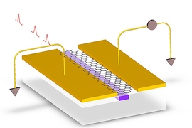
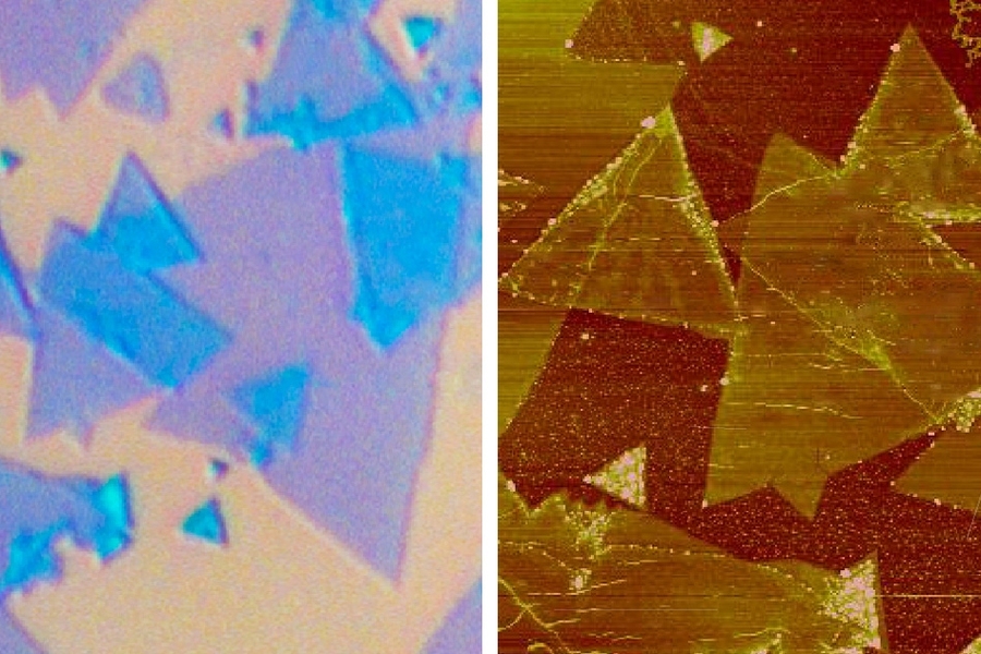
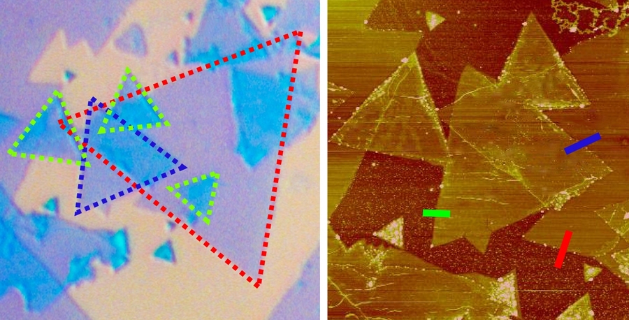
The MIT researchers tuned their emitters by depositing two layers of MoS2 on a silicon substrate. The top layers were rotated relative to the lower layers, and the degree of rotation determined the wavelength of the emitted light.
Ordinarily, MoS2 is a good light emitter only in monolayers, or atom-thick sheets. As Huang explains, that’s because the two-dimensional structure of the sheet confines the electrons orbiting the MoS2 molecules to a limited number of energy states.
MoS2, like all light-emitting semiconductors, is what’s called a direct-band-gap material. When energy is added to the material, either by a laser “pump” or as an electrical current, it kicks some of the electrons orbiting the molecules into higher energy states. When the electrons fall back into their initial state, they emit their excess energy as light.
In a monolayer of MoS2, the excited electrons can’t escape the plane defined by the material’s crystal lattice: Because of the crystal’s geometry, the only energy states available to them to leap into cross the light-emitting threshold. But in multilayer MoS2, the adjacent layers offer lower-energy states, below the threshold, and an excited electron will always seek the lowest energy it can find.
Mind the gap
So while the researchers knew that rotating the layers of MoS2 should alter the wavelength of the emitted light, they were by no means certain that the light would be intense enough for use in optoelectronics. As it turns out, however, the rotation of the layers relative to each other alters the crystal geometry enough to preserve the band gap. The emitted light is not quite as intense as that produced by a monolayer of MoS2, but it’s certainly intense enough for practical use — and significantly more intense than that produced by most rival technologies.
The researchers were able to precisely characterize the relationship between the geometries of the rotated layers and the wavelength and intensity of the light emitted. “For different twisted angles, the actual separation between the two layers is different, so the coupling between the two layers is different,” Huang explains. “This interferes with the electron densities in the bilayer system, which gives you a different photoluminescence.” That theoretical characterization should make it much easier to predict whether other transition-metal compounds will display similar light emission.
“This thing is something really new,” says Fengnian Xia, an assistant professor of electrical engineering at Yale University. “It gives you a new model for tuning.”
“I expected that this kind of angle adjustment would work, but I didn’t expect that the effect would be so huge,” Xia adds. “They get quite significant tuning. That’s a little bit surprising.”
Xia believes that compounds made from other transition metals, such as tungsten disulfide or tungsten diselenide, could ultimately prove more practical than MoS2. But he agrees that the MIT and RPI researchers’ theoretical framework could help guide future work. “They use density-functional theory,” he says. “That’s a kind of general theory that can be applied to other materials also.”