MIT has become an increasingly international institution, attracting top technical talent from all over the planet. But Michael Watts, who recently earned tenure in the Department of Electrical Engineering and Computer Science, is as local as they come.
Watts grew up in Hingham, Massachusetts, about 20 miles from Cambridge, working summers and vacations for his parents’ flooring and rug company, which his grandfather had founded. As a teen, he once had a job installing flooring at Draper Laboratory, which spun out from the lab of MIT aeronautical engineering professor Charles Stark Draper and has offices a few blocks away from the Kendall/MIT subway station.
At Hingham High School, Watts fell under the spell of a physics teacher named Charles Dirk. A former navy officer, Dirk “was a very excitable character,” Watts says. “If somebody didn’t get it, he would get red in the face.” But Watts responded well to Dirk’s teaching style, taking two classes with him and earning perfect scores on both the College Board’s physics achievement test and the advanced-placement physics exam. “Dirk was a teacher who definitely made a difference on many young minds, a unique character and gifted teacher,” Watts says.
For college, Watts says, “I wanted to stay local,” so he headed to Tufts University, in the Boston suburb of Medford, about a mile from the Cambridge border. He’d planned to study mechanical engineering, but Tufts had just opened a new center for the study of optoelectronics, or the integration of optical and electronic signal processing. A family friend who worked at Polaroid — which had its own optoelectronic research program — urged Watts to check it out.
Almost immediately, Watts was hooked. Optics, and particularly optoelectronics, would remain the theme of his studies and future research.
Cantabrigian
After graduating from Tufts in 1996, Watts got a job at Draper Lab, where he’d been laying floors just a few years earlier. He wasn’t the only member of the Draper technical staff without a graduate degree, but he was certainly in the minority. Nonetheless, he distinguished himself enough to attract the attention of Hermann Haus, an MIT Institute Professor and optics pioneer who was collaborating with some of the lab’s researchers. When, after three years at Draper, Watts applied to MIT to do a PhD in Haus’ group, Haus wrote one of his letters of recommendation.
Haus was working on what at the time was the cutting-edge field of silicon photonics. Many researchers were investigating other, more exotic semiconductors for use in optoelectronics. But silicon is, of course, the fundamental component of all modern computing devices. And there were reasons to believe that the combination of silicon and silicon dioxide, which was already used in commercial manufacturing processes, could yield very small optical components. Haus’ thinking was that if it should prove possible to build optical components from silicon, the component density and material compatibility would make it much easier and more affordable to integrate them with electronics.
One problem with silicon optical components was that they tended to work only with strongly polarized light — light whose waves are all oriented in the same direction. For both his master’s and his doctoral theses, Watts developed a photonic circuit that splits the polarization states of incoming light into two perpendicular components, then rotates one of them to align it with the other. Making silicon photonics “polarization independent” was essential to integrating them with existing optical-communication systems.
Decision points
One morning when he was a graduate student, Watts was walking down the street near his Boston apartment when he brushed shoulders with a young woman who looked a little like someone he’d last seen 10 years earlier — the daughter of some friends of his parents who also owned a flooring business, in New Hampshire. He turned and called after her: “Amy?” When she stutter-stepped, he called her name again, and they stopped to catch up. It turned out that she, too, was in a doctoral program, at the New England College of Optometry. The same spring that Watts graduated from MIT, he and Amy were married.
As graduation approached, Watts applied for two jobs: one at MIT’s Lincoln Laboratory and one at Sandia National Laboratories. “My research was going well,” Watts says, “so I decided to push that component first and figured if I decided later I wanted to teach I could do so after I had established myself in my field. I think it’s asking a lot to have faculty come in and have to build up a world-class research portfolio in a limited period of time while also learning how to teach, which by itself is a full-time job.”
Lincoln Lab was interested but had no openings in its silicon-photonics group. Sandia had a modern silicon fabrication facility, but no silicon-photonics group; it offered Watts the chance to build one. So he and Amy headed for New Mexico.
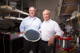
At Sandia, Watts managed to secure $200,000 in funding from the Defense Advanced Research Projects Agency (DARPA), a meager sum for research that requires as much high-tech prototyping as silicon photonics does. Nonetheless, Watts’ team was able to build most of the core components of a silicon-photonic platform, including a modulator that set a record for low power consumption and a high-speed switch, which together won an R&D100 award from R&D magazine. Five years after arriving at Sandia, Watts was running a $2-million-a-year research program.
Homecoming
But by this point, he and Amy had two small children, and traveling from New Mexico to visit two sets of grandparents in the Northeast was difficult and expensive. So again, Watts applied for two jobs, one at the State University of New York at Albany, which has access to the best semiconductor-manufacturing facilities in academia, and one at MIT. MIT was the one to give him an offer, and he accepted.
Back on campus, “I got a key to a small office, and I’m just looking at my four cinder-block walls, thinking, ‘What the hell do I do now?’” Watts says. “I realized I had completely hit the reset button.”
But the skills he’d developed at Sandia served him well. Within a year, he’d landed a $12 million grant from DARPA to develop integrated silicon optics and electronics. That meant, however, trying to get a new manufacturing facility — SUNY Albany’s, as it happened — up to speed on the custom 250-step fabrication process required to produce his silicon-photonic designs. “And the tenure clock was ticking,” Watts says. “Fortunately, I found a great partner, Dr. Coolbaugh, at SUNY, to help turn my ideas into reality.”
It took a few years to get going, but then the breakthroughs began coming in short order: the largest — by a few orders of magnitude — on-chip silicon phased array, which can steer light in different directions; another record-setting low-power modulator, which achieves state-of-the-art data rates; an on-chip erbium laser that can be built using standard silicon manufacturing techniques; and new methods for integrating optics and electronics on a single chip.
Watts’ work drew notice. Last year, after being granted tenure, he was named CTO of a consortium including MIT and SUNY Albany that secured a $110 million federal grant to support photonics manufacturing, part of the Obama administration’s manufacturing initiative.
In the meantime, Watts and his family landed back in Hingham, where his parents can help out with babysitting. His nine-year-old daughter, Samantha, is “incredibly good at art and design,” Watts says. “So she’s a little more artsy than I am.” At age six, his son William, on the other hand, “is very squarely engineer-minded,” Watts says. “Whenever we get on a boat or a plane, it’s, ‘How much horsepower does it have? How many gallons of fuel does it hold?’ He’s trying to measure it out.”