


MIT is a key player in a new $600 million public-private partnership announced today by the Obama administration to help strengthen high-tech U.S.-based manufacturing.
Physically headquartered in New York state and led by the State University of New York Polytechnic Institute (SUNY Poly), the American Institute for Manufacturing Integrated Photonics (AIM Photonics) will bring government, industry, and academia together to advance domestic capabilities in integrated photonic technology and better position the U.S. relative to global competition.
Federal funding of $110 million will be combined with some $500 million from AIM Photonics’ consortium of state and local governments, manufacturing firms, universities, community colleges, and nonprofit organizations across the country.
Technologies that can help to integrate photonics, or light-based communications and computation, with existing electronic systems are seen as a crucial growth area as the world moves toward ever-greater reliance on more powerful high-tech systems. What’s more, many analysts say this is an area that could help breathe new life into a U.S. manufacturing base that has been in decline in recent years.
The public-private partnership announced today aims to spur these twin goals, improving integration of photonic systems while revitalizing U.S. manufacturing. The consortium includes universities, community colleges, and businesses in 20 states. Six state governments, including that of Massachusetts, are also supporting the project.
MIT faculty will manage important parts of the program: Michael Watts, an associate professor of electrical engineering and computer science, will lead the technological innovation in silicon photonics. Lionel Kimerling, the Thomas Lord Professor in Materials Science and Engineering, will lead a program in education and workforce development.
“This is great news on a number of fronts,” MIT Provost Martin Schmidt says. “Photonics holds the key to advances in computing, and its pursuit will engage and energize research and economic activity from Rochester, New York, to Cambridge, Massachusetts, and beyond. MIT faculty are excited to contribute to this effort.”
An ongoing partnership
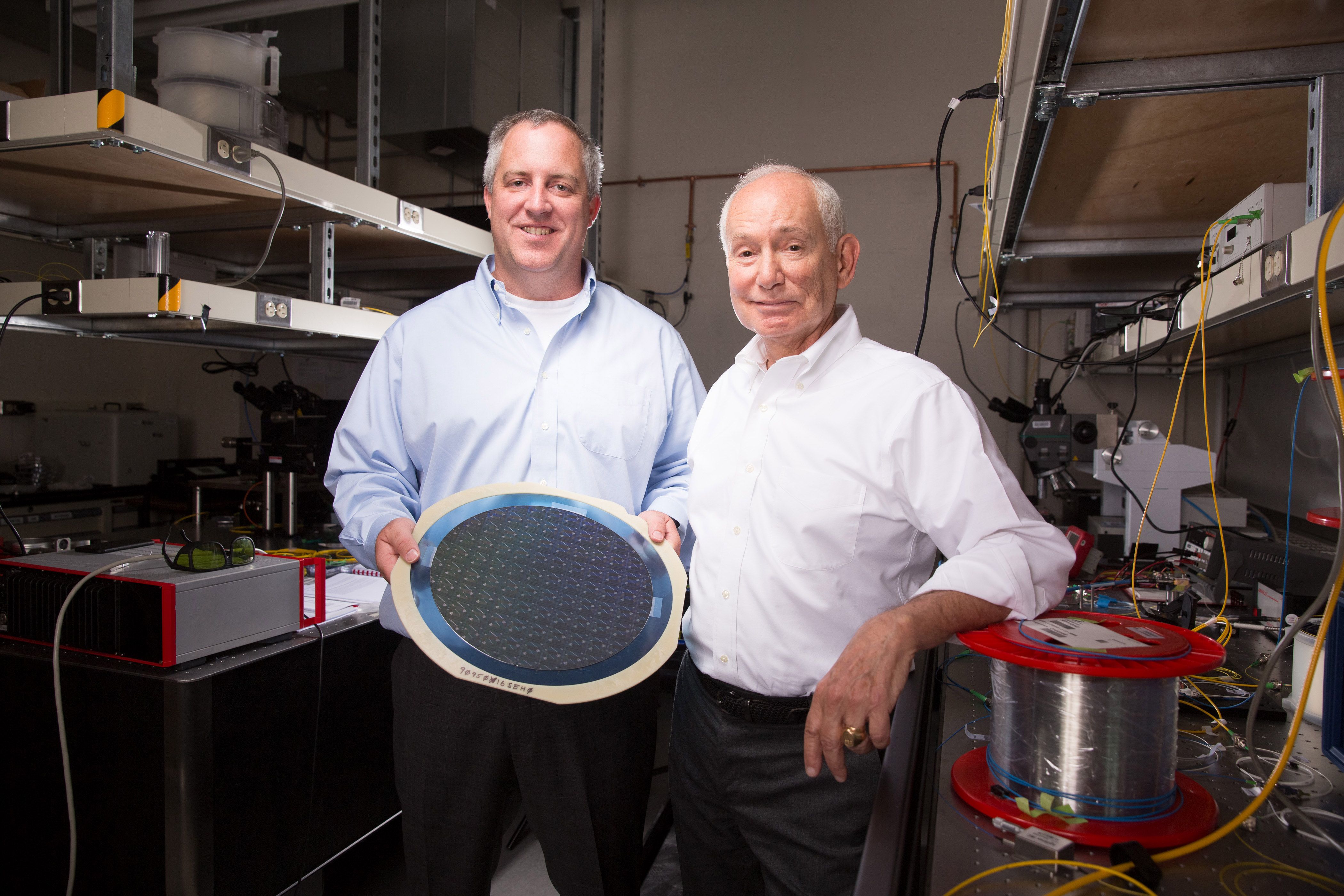
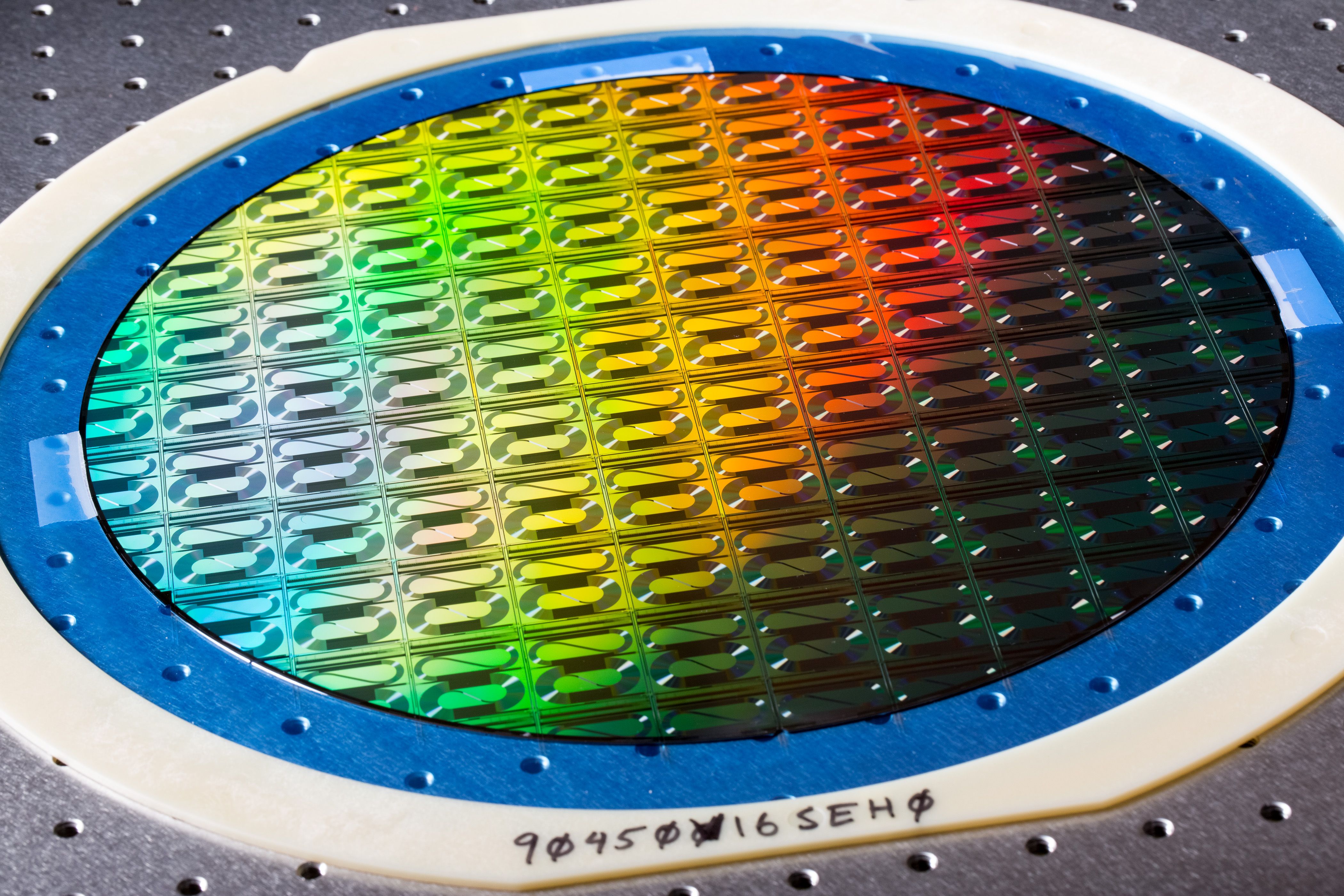
MIT’s existing collaboration with SUNY Poly led to the first complete 300-millimeter silicon photonics platform, Watts says. That effort has led to numerous subsequent advances in silicon photonics technology, with MIT developing photonic designs that SUNY Poly has then built in its state-of-the-art fabrication facility.
Photonic devices are seen as key to continuing the advances in computing speed and efficiency described by Moore’s Law — which may have reached their theoretical limits in existing silicon-based electronics, Kimerling says. The integration of photonics with electronics promises not only to boost the performance of systems in data centers and high-performance computing, but also to reduce their energy consumption — which already accounts for more than 2 percent of all electricity use in the U.S.
Kimerling points out that a single new high-performance computer installation can contain more than 1 million photonic connections between hundreds of thousands of computer processor units (CPUs). “That’s more than the entire telecommunications industry,” he says — so creating new, inexpensive, and energy-efficient connection systems at scale is a major need.
The integration of such systems has been progressing in stages, Kimerling says. Initially, the conversion from optical to electronic signals became pervasive at the network level to support long-distance telecommunication, but it is now moving to circuit boards, and will ultimately go to the level of individual integrated-circuit chips.
“Europe is ahead in industry coordination right now,” following a decade of government investment, Kimerling says. This new U.S. initiative, he says, is “one of the first of this kind in the U.S., and the bet is that the innovation and research here, combined with the manufacturing capability, will allow our companies to really take off.”
Leadership in technological innovation
Within the new alliance, MIT will lead technological innovation in silicon photonics. That task will be managed by Watts.
The evolving integration of photonics and electronics will have a great impact on many different technologies, Watts says. For example, LIDAR systems — similar to radar, but using light beams instead of radio waves — have great potential for collision-avoidance systems in cars, since they can provide greater detail than radar or sonar. Watts has worked to develop single-chip LIDAR devices, which could eliminate the moving parts in existing devices — such as tiny gimbaled mirrors used to direct the light beams in a scanning pattern — replacing them with fixed, electrically steerable phased-array systems, like those now used for cellphone tower antennas.
“LIDAR systems that exist today are both bulky and expensive, because they use mechanically scanned lasers,” Watts says. But doing the same thing at the nanoscale, using phased-array systems on a chip, could drastically reduce size and cost, providing high-resolution, chip-scale, 3-D imaging capabilities that do not exist today, he says.
There are many other areas where integration of photonics and electronics could lead to big advances, including in biological and chemical sensors that could have greater sensitivity than existing electronic versions, and in new kinds of medical imaging systems, such as optical coherent tomography.
“The goal of this initiative is to lower the barriers to entry in this field for U.S. companies,” Watts says. It is intended to function much like a major public-private initiative that helped pave the way, decades ago, for the development of electronic chip manufacturing in the U.S.
Significant photonic chip manufacturing capabilities have been developed at SUNY Poly, in Albany, New York. That facility has already made the world’s largest silicon-based photonic circuit, a chip designed at MIT, and built using industry-standard 300-millimeter-wide silicon wafers, Watts says.
Contributions in education and training
MIT will also host AIM Photonics’ program in education and workforce development, which Kimerling will direct. This will include developing educational materials — ranging from K-12 through continuing education — to prepare future employees for this emerging industry, including teaching on the design of integrated photonic devices. MIT will also lead workforce development, with an emphasis on including veterans, underrepresented minorities, and other students, by developing a variety of materials to teach about the new technologies.
MIT will work to support internships, apprenticeships, and other forms of hands-on training in a national network of industry and university partners. The effort will also support an industry-wide roadmap to help align the technology supply chain with new manufacturing platforms.
Kimerling says that a significant issue in developing a robust photonics industry is the need to develop a trained workforce of people who are familiar with both electronics and optical technology — two very different fields. Educational programs that encompass these disparate fields “are important, and don’t exist today in one organization,” he says.
One expected impact of the new initiative is the development of a corridor along Interstate 90, from Boston to Rochester, New York, of industrial firms building on the base of new technology to develop related products and services, much as Silicon Valley emerged in California around companies such as Intel and their chip-making technology.
Other major members of AIM Photonics include the University of Arizona, the University of Rochester, and the University of California at Santa Barbara. In addition to the Department of Defense, federal funding for the project will come from the National Science Foundation, the Department of Energy, the National Institute for Standards and Technology, and NASA.
Roots in the Advanced Manufacturing Partnership
Today’s news flows from the work of the Advanced Manufacturing Partnership (AMP), a White House-led effort begun in 2011 with the aim of bringing together industry, universities, and the federal government to identify and invest in key emerging technologies, with the idea of stoking a “renaissance in American manufacturing.”
AMP was inaugurated with former MIT President Susan Hockfield as co-chair; MIT President L. Rafael Reif subsequently served in that same capacity as part of “AMP 2.0.” Those groups’ work led to President Barack Obama’s commitment to establish a National Network of Manufacturing Innovation, to consist of linked institutes such as the one announced today.
“Massachusetts’ strong role in the AIM Photonics team stems from a collaboration involving MIT and many other partner organizations across the Commonwealth: universities, community colleges, and large and small manufacturers throughout the integrated photonics supply chain,” says Krystyn Van Vliet, a professor of materials science and engineering and biological engineering, and MIT faculty lead for AMP 2.0. “The support of Gov. Charlie Baker and Secretary of Housing and Economic Development Jay Ash was key to the success of the AIM Photonics team, and we appreciate their efforts. This manufacturing institute will help Massachusetts inspire and prepare the next generation of integrated photonics manufacturing careers, businesses, and leaders.”
“Today’s announcement is a testament to the outstanding team of industrial and academic leaders assembled by AIM Photonics and its plan to establish the U.S. as a global leader in this emerging technology,” says Michael Liehr, AIM CEO and SUNY Poly executive vice president of innovation and technology and vice president of research. “This would not have been possible without the critical support of Gov. Andrew Cuomo, whose pioneering leadership in establishing New York state’s globally recognized, high-tech R&D ecosystem has enabled historic economic growth and innovation and secured our partnership with the state of Massachusetts. SUNY Poly is excited to be working with partners such as MIT on this initiative, which will be truly transformational for both the industry and the nation.”