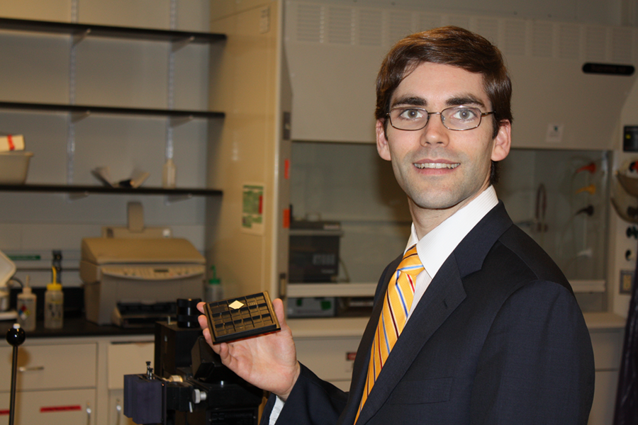
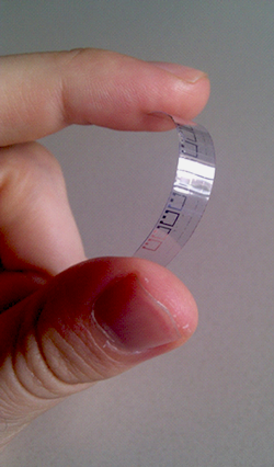
Flexible transparent displays and skin patches that act as sensors are among the many new devices based on two-dimensional quantum materials such as graphene and molybdenum disulfide that foretell a 40- to 50-year run similar to the silicon-based computer revolution, says Tomás Palacios, associate professor of electrical engineering and computer science at MIT.
"Thanks to new quantum properties observable at room temperature, we can come up with new applications. That's what makes quantum really exciting," he says. Palacios will present his recent work on memory cells, analog to digital converters and ring oscillators at the Materials Day Symposium on Wednesday, Oct. 14, in MIT's Kresge Auditorium. He envisions a future of electronics everywhere, or ubiquitous electronics.
"We are working on developing graphene-based devices that show quantum hall effect at room temperature in order to do single-photon detection for quantum communications as well as extremely high resolution metrology to make GPS work inside buildings," adds Palacios, who directs both the MIT/MTL Gallium Nitride Energy Initiative and the MIT/MTL Center for Graphene Devices and 2D Systems.
"The beauty of these materials is that they are extreme," Palacios explains. "There is nothing thinner, there is nothing stronger. There is nothing where electrons can go faster. These extreme unique properties give us new flexibility when designing devices and systems."
"We are starting the semiconductor revolution again; it's like today was 1960. We have a 40-, 50-year run in front of us to take full advantage of these new materials and the new generation of circuits and microsystems that these materials enable," Palacios says.
The theme of this year's Materials Day Symposium and Poster Session is "Quantum Materials," and it is being held in conjunction with the Center for Integrated Quantum Materials (CIQM) annual meeting. CIQM, which is supported by National Science Foundation Grant No. DMR-1231319, is a collaboration between Harvard University, MIT, Howard University, and the Museum of Science in Boston.
Materials Day speakers will present their latest insights into applying quantum phenonema to understanding basic science, developing new materials and creating new computers, sensors, energy and communication devices:
• Daniel Twitchen, chief technology officer for Element Six, will report on his firm's progress using chemical vapor deposition (CVD) and other mechanical and chemical methods to create synthetic diamonds for high-power optics applications such as infrared imaging and integrated photonics. He will also discuss controlling optical signals at single-photon level in single-crystal CVD diamond using nanocavities and waveguides for applications in quantum optics and magnetic sensing.
• Gary L. Harris, dean of the Howard University Graduate School, will present his use of silicon carbide as a substrate for epitaxially growing high-quality diamond by nanodiamond seeding. Harris is developing new diamond applications using nitrogen, silicon, and germanium as quantum dopants. Harris also is professor of electrical and computer engineering as well as associate provost for research and graduate studies at Howard. He is a co-principal investigator for CIQM.
• George Bourianoff, senior principal engineer in components research at Intel, will present an update on synchronization of coupled oscillator arrays for association and reservoir computing with arrays of quantum dots or magnetic skyrmions.
• Pablo Jarillo-Herrero, the Mitsui Career Development Associate Professor of Physics at MIT, will describe his group's efforts in the area of quantum electronic transport and optoelectronics with van der Waals heterostructures, with examples ranging from the opening of a bandgap in graphene to the thinnest photodetectors, solar cells, and LEDs based on transition metal dichalcogenides.
• Amir Yacoby, professor of physics at Harvard University, will talk about his use of nitrogen vacancy center-based magnetometry to explore condensed matter physics. Yacoby has detected the spin-wave magnetic field at about 50 nanometers from a ferromagnetic microdisc. Yacoby also will demonstrate direct imaging of skyrmionic spin textures in magnetic thin films, which are of great interest for memory devices.
• Nuh Gedik, the Lawrence C. (1944) and Sarah W. Biedenharn Career Development Associate Professor of Physics at MIT, will discuss his work on topological insulators, which possess exceptional conducting electronic states on their surface yet do not conduct electricity in their bulk. His work on these materials revealed an exotic hybrid state between electrons and light, which was predicted theoretically but had never been observed in solids before. Gedik will describe recent experiments using ultrashort laser pulses to probe and control properties of the topological surface states and capture femtosecond movies of their electronic energy bands. Understanding and characterizing unique properties of these materials can lead to novel applications such as current induced magnetization or extremely robust quantum memory bits.
Electronics everywhere
Palacios believes the coming era of electronics everywhere will be enabled by additive manufacturing. "What we have done during the last year is modify a 3-D printer to be able to print at the same time structural materials like any other 3-D printer as well as electronic, 2-D materials, which we are using to make all kinds of sensors, energy harvesters, as well as a little bit of logic that we can embed inside any object we can print," he says.
Quantum materials are also ideal for large-area, highly distributed systems such as sensor networks to cover entire surfaces of airplanes or spacecraft. "To enable that network of sensors, you need very large area electronics that can be deployed over very textured surfaces," Palacios says. "For that, I believe, these materials are just ideal, because you can make them almost like you print newspapers in a roll-to-roll basis, and you can fabricate devices at very low cost. They may not have very high performance, but you may not need very fast devices to know the structural integrity of an aircraft, for example."
The first applications to incorporate these new materials and devices will likely be ones that cannot be done with conventional materials. From that point of view, large area distributed systems are likely to be one of the first with uses such as monitoring the structural integrity of bridges, highways and other infrastructure. "It will grow from there," he suggests.
Another advantage of these two-dimensional, quantum materials — some as thin as a single-atom to three atoms in thickness — is their ability to be folded over and over again. Inspired by biology, in particular organelles and their highly folded proteins, Palacios is pursuing a new line of research to create highly folded electronic devices. "The performance density, the amount of functionality, that we can get from a cell is a lot higher than the performance density that we can get from a silicon-based chip," Palacios explains "The smallest silicon-based system we have is probably a few cubic millimeters, while a cell is able to integrate energy harvesting, communication, chemical sensing, a little bit of processing, all into 10 cubic microns. The difference between silicon-based electronics and biology is folding, to be able to access the third dimension." Along with researchers at Harvard and the University of Southern California, Palacios leads an Air Force-funded MURI to make two-dimensional circuits, then fold them over and over again to mimic the structure of proteins.
"Five years from now, when the program is over, we will have these vials with basic building blocks of highly folded electronic circuits, that we will be able to combine in the same way that nature is able to combine biological organelles. So I'm very, very excited at this new wave of devices and systems enabled by engineering the folding of these on two-dimensional materials," he says.
The Materials Day Symposium, will be held from 8:45 a.m. to 3:30 p.m. on Wednesday, Oct. 14, in MIT's Kresge Auditorium. Immediately following, the poster session takes place from 3:30 to 5:30 p.m. in La Sala de Puerto Rio, 2nd Floor, in the Stratton Student Center.
The CIQM annual meeting takes place from 8:50 a.m. to 4:45 p.m., Thursday, Oct. 15, in La Sala de Puerto Rico, 2nd Floor, Stratton Student Center, followed by the poster session from 4:45 to 6:30 p.m.
The Materials Processing Center (MPC) celebrated 35 years of service to the MIT faculty and materials research community on Feb. 1. As an interdisciplinary center within MIT's School of Engineering, MPC serves about 60 researchers in both the School of Engineering and the School of Science, assists in drafting proposals and administering grants, and provides industrial outreach and communications. The MPC also helps faculty to organize interdisciplinary teams for large grants, new initiatives, and development of new research centers.
