Everyday materials like copper and gold, both chemical elements, are widely used for their ability to conduct electricity. Other materials like rubber or polyvinylchloride are used for their ability to block, or insulate, electricity. In recent years researchers have identified a new class of materials called topological insulators, which combine both functions, for example, insulating in the bulk while conducting electricity freely along their surfaces.
Nuh Gedik, an associate professor of physics, is exploring these new materials using a variety of laser-driven techniques to understand their unique qualities, which are attributable to quantum phenomena, a regime marked by a limited number of mutually exclusive states, unlike the seemingly continuous behavior of materials at the macroscale.
Opening a bandgap
While it was already known that laser light with energy greater than the bandgap could excite electrons in material and change their electronic state, Gedik's team discovered in the past two years that even laser light with smaller energy could produce unexpected interactions that also change electronic properties. By shining light and hybridizing electrons with photons, the researchers created new hybrid states known as Floquet-Bloch states.
"If you tune the energy of the light below a specific absorption, so that normally it should not be absorbed by the solid, light should just go through without doing much, now it turns out that something else happens. Electrons inside the material hybridize with the photons of the light beam, and they produce new states that are not there just with the light, or just with the electrons. It's only there when the two are there," he says. And this coupling, or hybridization, modifies the electronic energy states inside the solid. Of particular relevance to electronics, the hybridization opened a bandgap in the material under study, bismuth selenide (Bi2Se3).
"The goal of my research is to both understand and control the properties of these materials with light. The eventual dream is engineering new materials, or novel material properties using light excitation," Gedik says.
Gedik will speak about his research on topological insulators at the Materials Day Symposium, on Wednesday, Oct. 14, in MIT's Kresge Auditorium. This year's theme is quantum materials. "I am very much looking forward to the Materials Day Symposium and honored to be speaking about our research," Gedik says. "It is a unique event that brings industry and academia together."
Overcoming limitations
Electrons and quantum events move so fast it would be impossible to take a picture of them using light the way a camera captures everyday life. Think of a camera taking a photo at a slow shutter speed of a person running, Gedik suggests. The picture will be blurry because the person moved during the length of the exposure. Put the person running in a darkened room and set off a very fast flash of light and the camera will capture an image of the person at only the moment when the flash is on, so the image will be sharp. "Exactly the same problem happens when you try to time resolve, or take pictures of, electrons," Gedik explains. "No matter how fast your camera is, the fastest camera you can think of in the world, it wouldn't be able to capture the relevant motion because electrons move very fast. The time scale we're talking about is a billionth of a millionth of a second — a femtosecond."
Gedik has developed time-resolved techniques to overcome these limitations by using ultrafast laser pulses, first sending a femtosecond pump laser pulse to initiate a process, followed by a probe laser pulse after some time delay to measure the relaxation of the material. "By taking snapshots with the probe beam at different times after the arrival of the pump beam, one can produce a "movie" of this process. Our detectors are slow, but we only capture the motion during that short pulse of light. From this we can actually deduce, and understand what must have happened," he says.
"What I also like about our techniques is that they are non-contact," Gedik says. "We don't even touch the sample. We send the light pulse and from the reflection or transmission that comes out or from the electrons that are ejected by light, we can deduce something ... Without touching it, we can actually learn so much."
Measuring energy and momentum of electrons in complex materials such as topological insulators is one of a half-dozen or so experimental approaches used in Gedik's group. This technique allows taking snapshots of how electronic energy levels change with the electron momentum, which is crucial for understanding material properties. Besides taking a snapshot, Gedik group can also visualize dynamics of how electrons scatter. They do this by first exciting electrons with another laser pulse and then record the energy and momentum of the electrons at different times after the light excitation. Besides making a "movie" of the electronic energy levels, they can also probe the motion of the ions in the solid (lattice) or the spins of the electrons. "In order to probe the dynamics of the lattice, we use the diffraction of a high-energy electron probe. Or if we want to look at the spins of the electrons, we actually utilize polarization of the light," he says.
Polarization effects
Light is an electromagnetic wave with both linear and angular momentum, Gedik explains. Normally its electric field oscillates in a straight line perpendicular to the direction of propagation of the light. But it is possible to create light beams for which the direction of electric field continuously rotates on a circle, which is known as circularly polarized light. Depending on the direction of rotation, it has the effect of giving the light a distinctive orientation akin to left-handedness or right-handedness.
This property of the light allows it couple to the angular momentum of electrons, Gedik says. Working under Gedik, graduate student Edbert Jarvis Sie and colleagues used this effect of circularly polarized light to demonstrate that it could be used to control the energy level of the electron energy valleys paving the way for a new form of electronics called valleytronics.
Using the techniques of measuring electron energy and momentum to quantify electronic states, the researchers found they could change theses states by changing the polarization of the light. "This paper is an example in which, by using right circularly polarized or left circularly polarized light, we actually address two different electronic valleys in the material," Gedik explains. These particular experiments did not have to be done in vacuum, Sie says. The researchers experimented on an atomically thin layer of tungsten disulfide (WS2), a material that is used commercially in its bulk form as a lubricant. Professor of electrical engineering and computer science Jing Kong and Yi-Hsien Lee, who is a Kong research group alumnus, provided the tungsten disulfide monolayer. Gedik group alumnus James McIver, who is now a postdoc at Max Planck Institute for the Structure and Dynamics of Matter in Germany, also contributed to the research.
In their experiment, the MIT researchers showed that if you plot the energy of the electrons as a function of their momentum, there are two energetic minimums, or valleys, in which electrons will gather. "These are two points in the momentum space that we will call K and K prime (K')," Gedik explains. Under normal conditions, electrons will be balanced in these two valleys. But subjecting the material to circularly polarized light shifts one valley in energy with respect to the other one, tipping the balance to push more of the electrons into one valley instead of the other. "[In] this material, because of a symmetry that it has, the two valleys automatically have the same energy. We use this intense light pulse to break that symmetry and shift one valley with respect to the other one," Gedik says. Current electronic devices work by moving electrons based on their charge, but future versions may be based on controlling their spin (spintronics) or this newly discovered valley segregation (valleytronics).
The Gedik group, in collaboration with Professor Liang Fu, also proposed a fascinating idea of making a topological phase using this experiment. "By turning on the laser light, we can have a topological insulator; by turning it off, we can have back our semiconductor system. Because this material has the valley index, which is unique, then we can have this sort of valley-specific topological insulator," Sie explains. Because there are two valleys, "We can make the topological phase at one valley and a normal semiconductor phase at the other valley or vice versa by changing the laser polarization." Edbert Sie and his colleagues are currently working to realize this theoretical proposal experimentally.
Alternative to powerful magnets
Using powerful laser light isn't the only way to manipulate electronic valleys in materials such as tungsten disulfide, which are known as transition metal dichalcogenides. But light is much more efficient at accomplishing the task than the alternative method of using a powerful magnetic field. "The magnetic field that you would require, to give you the same effect, is tens of tesla, which is not practical in the lab," Gedik says.
A remaining question is how fast these valleys revert to their balanced natural state after they are shifted by applying a polarized laser light, he says.
Combining techniques
Different experimental approaches yield different insights into the electronic behavior of materials such as topological insulators, graphene, and related ultrathin materials. Electron diffraction gives insight into lattice structure, which is the arrangement of the atomic ions inside the solid, while other techniques yield data about electron energy and momentum, electronic band structure, or electron spin. "What's unique about our lab is we have combined these different techniques. ... The idea is [we] make all these different movies and bring them together and understand what's happening inside," he says.
There are currently seven graduate students and four postdoctoral associates in Gedik's research group. They work collaboratively on the often complex experimental setups. For example, graduate students Edbert Sie and Fahad Mahmood recently did complementary experiments. "The nice thing is that on the same material, for example, tungsten disulfide, Fahad was doing an experiment using his optical technique and Edbert was doing an experiment using a separate optical technique, but they were kind of looking at the same phenomena, and it's a lot of fun to kind of discuss these different experiments and how we can converge into one picture," Gedik says.
Sie commends Gedik for his easy accessibility to graduate students, postdocs and undergrads alike. "A lot of the success of the work is not only fortuitous but also because of the great mentorship of the advisor. Everybody would agree with me that Nuh has been an excellent advisor. Although he is busy with his commitments of teaching or giving talks to the whole world, he will always have time for us," Sie says. "So we are very thankful that he can share his time and also his ideas with all of us. That is something that Nuh cannot say, but everybody will agree with me."
Probing Cooper pairs
Gedik's lab also conducts experiments in superconductivity, in particular, trying to understand why negatively charged electrons that normally repel each other sometimes are attracted to each other forming what is known as a Cooper pair. In particular, they are working on understanding why electrons pair themselves in a newer class of superconductors known as high transition temperature superconductors. "Nobody knows why electrons attract each other or why they are making pairs in these superconductors," Gedik says.
"The simplest experiment we could do is we come with the first light pulse, and we actually break these pairs, but then these electrons because they really want to be in pairs, in a very fast time scale, they come back and they make pairs again," Gedik explains. "We kind of watch as they pair, and try to understand why is it that they pair, number one, and number two, when we break these pairs, the electrons give this energy to something else. That something else is probably the glue that binds them together. By watching movies we also look for that glue that actually binds them together."
The researchers found that in some materials, besides electrons pairing themselves, other electrons were forming a charge density wave, meaning their density was being modulated in space, Gedik says. Graduate student Mahmood conducted experiments that showed these charge density waves are real but last for no more than two picoseconds and are gone. "This was kind of the very first observation of a fluctuating charge density wave in that particular material, and we were able to make some connections to how it's related to superconductivity as well," Gedik says.
"This order is fluctuating," Mahmood adds, "so sometimes electrons want to pair together in superconductivity and sometimes they want to be part of this other charge density wave. ... Because it lives for a very short time, it is very difficult to see this with other techniques. By observing it so quickly, we were able to detect it and can actually make predictions on how it actually competes with superconductivity, so that's sort of the main advance of that particular work."
Classroom examples
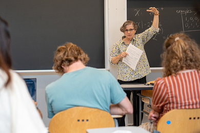
For the past three years, Gedik has taught 8.02 (Electricity and Magnetism), a class made up of mostly physics majors, in which electromagnetic waves and light are a major focus. "Frequently, I would be giving them examples from our lab," he says. For example, students are shown how to compare the value of the electric field coming from sunlight to the electric field at the focal point of the laser beam in the Gedik Lab. When Gedik's most powerful lasers are focused in a tight spot in air, the electric field is so big that it ionizes molecules in the air, thus creating artificial lightning. The laser has a repletion rate of 5 kilohertz (kHz), so you also hear a sound at 5 kHz due to pressure waves created in air, he says.
In the lab, however, "We don't want to send too strong a light pulse into a material because you can damage the stuff if the light pulse is too intense," he says.
Gedik, 35, and his wife, Reyhan, have a 4-year-old son named Bahadir. Trying to explain to his son where the sun goes at night is more difficult than writing a technical paper, he says.
Gedik won tenure in June 2015. He received his BS in physics in 1998 from Bogazici University in Istanbul, Turkey, and his PhD in physics in 2004 from the University of California at Berkeley. Following a postdoctoral appointment at Caltech, he joined the faculty of MIT's Department of Physics in 2008. Gedik also received a National Science Foundation CAREER Award, an Alfred P. Sloan Fellowship, and the Moore Experimental Investigator Award in Quantum Materials.


