A team of MIT researchers has used a novel material that’s just a few atoms thick to create devices that can harness or emit light. This proof-of-concept could lead to ultrathin, lightweight, and flexible photovoltaic cells, light emitting diodes (LEDs), and other optoelectronic devices, they say.
Their report is one of three papers by different groups describing similar results with this material, published in the March 9 issue of Nature Nanotechnology. The MIT research was carried out by Pablo Jarillo-Herrero, the Mitsui Career Development Associate Professor of Physics, graduate students Britton Baugher and Yafang Yang, and postdoc Hugh Churchill.
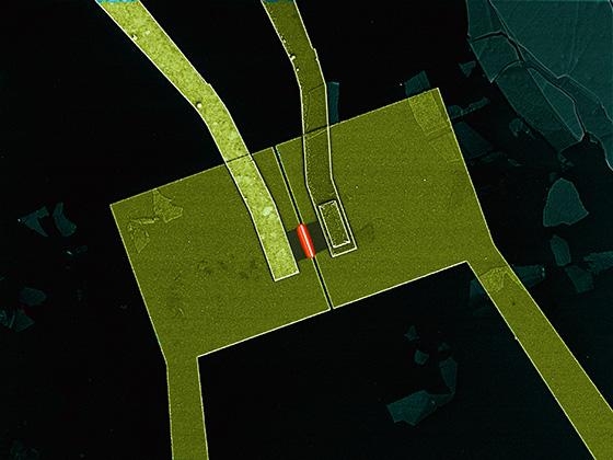
The material they used, called tungsten diselenide (WSe2), is part of a class of single-molecule-thick materials under investigation for possible use in new optoelectronic devices — ones that can manipulate the interactions of light and electricity. In these experiments, the MIT researchers were able to use the material to produce diodes, the basic building block of modern electronics.
Typically, diodes (which allow electrons to flow in only one direction) are made by “doping,” which is a process of injecting other atoms into the crystal structure of a host material. By using different materials for this irreversible process, it is possible to make either of the two basic kinds of semiconducting materials, p-type or n-type.
But with the new material, either p-type or n-type functions can be obtained just by bringing the vanishingly thin film into very close proximity with an adjacent metal electrode, and tuning the voltage in this electrode from positive to negative. That means the material can easily and instantly be switched from one type to the other, which is rarely the case with conventional semiconductors.
In their experiments, the MIT team produced a device with a sheet of WSe2 material that was electrically doped half n-type and half p-type, creating a working diode that has properties “very close to the ideal,” Jarillo-Herrero says.
By making diodes, it is possible to produce all three basic optoelectronic devices — photodetectors, photovoltaic cells, and LEDs; the MIT team has demonstrated all three, Jarillo-Herrero says. While these are proof-of-concept devices, and not designed for scaling up, the successful demonstration could point the way toward a wide range of potential uses, he says.
“It’s known how to make very large-area materials” of this type, Churchill says. While further work will be required, he says, “there’s no reason you wouldn’t be able to do it on an industrial scale.”
In principle, Jarillo-Herrero says, because this material can be engineered to produce different values of a key property called bandgap, it should be possible to make LEDs that produce any color — something that is difficult to do with conventional materials. And because the material is so thin, transparent, and lightweight, devices such as solar cells or displays could potentially be built into building or vehicle windows, or even incorporated into clothing, he says.
While selenium is not as abundant as silicon or other promising materials for electronics, the thinness of these sheets is a big advantage, Churchill points out: “It’s thousands or tens of thousands of times thinner” than conventional diode materials, “so you’d use thousands of times less material” to make devices of a given size.
In addition to the diodes the team has produced, the team has also used the same methods to make p-type and n-type transistors and other electronic components, Jarillo-Herrero says. Such transistors could have a significant advantage in speed and power consumption because they are so thin, he says.
Kirill Bolotin, an assistant professor of physics and electrical engineering at Vanderbilt University, says, "The field of two-dimensional materials is still at its infancy, and because of this, any potential devices with well-defined applications are highly desired. Perhaps the most surprising aspect of this study is that all of these devices are efficient. ... It is possible that devices of this kind can transform the way we think about applications where small optoelectronic elements are needed."
The research was supported by the U.S. Office of Naval Research, by a Packard fellowship, and by a Pappalardo fellowship, and made use of National Science Foundation-supported facilities.