As the United States seeks to reinvigorate its job market and move past economic recession, MIT News examines manufacturing’s role in the country's economic future through this series on work at the Institute around manufacturing.
To make a silicon solar cell, you start with a slice of highly purified silicon crystal, and then process it through several stages involving gradual heating and cooling. But figuring out the tradeoffs involved in selecting the purity level of the starting silicon wafer — and then exactly how much to heat it, how fast, for how long, and so on through each of several steps — has largely been a matter of trial and error, guided by intuition and experience.
Now, MIT researchers think they have found a better way.
An online tool called “Impurities to Efficiency” (known as I2E) allows companies or researchers exploring alternative manufacturing strategies to plug in descriptions of their planned materials and processing steps. After about one minute of simulation, I2E gives an indication of exactly how efficient the resulting solar cell would be in converting sunlight to electricity.
One crucial factor in determining solar cell efficiency is the size and distribution of iron particles within the silicon: Even though the silicon used in solar cells has been purified to the 99.9999 percent level, the tiny remaining amount of iron forms obstacles that can block the flow of electrons. But it’s not just the overall amount that matters; it’s the exact distribution and size of the iron particles, something that is both hard to predict and hard to measure.
Graduate student David Fenning, part of the MIT team behind I2E, compares the effect of iron atoms on the flow of electrons in a solar cell to a group of protesters in a city: If they gather together in one intersection, they may block traffic at that point, but cars can still find ways around and there is little disruption. “But if there’s one person in the middle of every intersection, the whole city could shut down,” he says, even though it’s the same number of people.
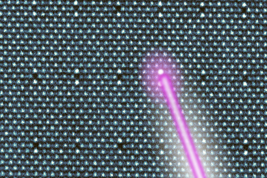
A team led by assistant professor of mechanical engineering Tonio Buonassisi, including Fenning, fellow graduate student Douglas Powell and collaborators from the Solar Energy Institute at Spain's Technical University of Madrid, found a way to use basic physics and a detailed computer simulation to predict exactly how iron atoms and particles will behave during the wafer-manufacturing process. They then used a highly specialized measurement tool — an X-ray beam from a synchrotron at Argonne National Laboratory — to confirm their simulations by revealing the actual distribution of the particles in the wafers.
“High-temperature processing redistributes the metals,” Buonassisi explains. Using that sophisticated equipment, the team took measurements of the distribution of iron in the wafer, both initially and again after processing, and compared that with the predictions from their computer simulation.
Free of charge, the I2E website has been online since July, and users have already carried out approximately 2,000 simulations. The details of how the system works and examples of industrial impact will be reported soon in a paper in the trade journal Photovoltaics International. The U.S. Department of Energy, which supported the research, has also reported on the new tool in an entry that will be posted on the agency’s blog.
Already, Powell says, I2E has been used by “research centers from around the world.”
Without the tool, there are simply too many possible variations to test, so people end up selecting the best from a small number of choices. But with I2E, Buonassisi says, “you can look for the global optimum” — that is, the best possible solution for a given set of requirements. “We can really speed up the innovation process,” he says.
Fenning says that companies generally “can’t afford to do these large experiments” needed to figure out the best process for a given application. The physics of what goes on inside the wafer during the processing is complex, he says: “There are a number of competing mechanisms that cloud the picture of exactly what is going on,” which is why developing the simulation was a long and complex process.
Now that the simulation tool is available, Fenning says, it helps manufacturers balance product quality against production time. Because there are so many variations in the supplies of starting material, he says, “it’s a constantly evolving problem. That’s what makes it interesting.”
To make a silicon solar cell, you start with a slice of highly purified silicon crystal, and then process it through several stages involving gradual heating and cooling. But figuring out the tradeoffs involved in selecting the purity level of the starting silicon wafer — and then exactly how much to heat it, how fast, for how long, and so on through each of several steps — has largely been a matter of trial and error, guided by intuition and experience.
Now, MIT researchers think they have found a better way.
An online tool called “Impurities to Efficiency” (known as I2E) allows companies or researchers exploring alternative manufacturing strategies to plug in descriptions of their planned materials and processing steps. After about one minute of simulation, I2E gives an indication of exactly how efficient the resulting solar cell would be in converting sunlight to electricity.
One crucial factor in determining solar cell efficiency is the size and distribution of iron particles within the silicon: Even though the silicon used in solar cells has been purified to the 99.9999 percent level, the tiny remaining amount of iron forms obstacles that can block the flow of electrons. But it’s not just the overall amount that matters; it’s the exact distribution and size of the iron particles, something that is both hard to predict and hard to measure.
Graduate student David Fenning, part of the MIT team behind I2E, compares the effect of iron atoms on the flow of electrons in a solar cell to a group of protesters in a city: If they gather together in one intersection, they may block traffic at that point, but cars can still find ways around and there is little disruption. “But if there’s one person in the middle of every intersection, the whole city could shut down,” he says, even though it’s the same number of people.
A team led by assistant professor of mechanical engineering Tonio Buonassisi, including Fenning, fellow graduate student Douglas Powell and collaborators from the Solar Energy Institute at Spain's Technical University of Madrid, found a way to use basic physics and a detailed computer simulation to predict exactly how iron atoms and particles will behave during the wafer-manufacturing process. They then used a highly specialized measurement tool — an X-ray beam from a synchrotron at Argonne National Laboratory — to confirm their simulations by revealing the actual distribution of the particles in the wafers.
“High-temperature processing redistributes the metals,” Buonassisi explains. Using that sophisticated equipment, the team took measurements of the distribution of iron in the wafer, both initially and again after processing, and compared that with the predictions from their computer simulation.
Free of charge, the I2E website has been online since July, and users have already carried out approximately 2,000 simulations. The details of how the system works and examples of industrial impact will be reported soon in a paper in the trade journal Photovoltaics International. The U.S. Department of Energy, which supported the research, has also reported on the new tool in an entry that will be posted on the agency’s blog.
Already, Powell says, I2E has been used by “research centers from around the world.”
Without the tool, there are simply too many possible variations to test, so people end up selecting the best from a small number of choices. But with I2E, Buonassisi says, “you can look for the global optimum” — that is, the best possible solution for a given set of requirements. “We can really speed up the innovation process,” he says.
Fenning says that companies generally “can’t afford to do these large experiments” needed to figure out the best process for a given application. The physics of what goes on inside the wafer during the processing is complex, he says: “There are a number of competing mechanisms that cloud the picture of exactly what is going on,” which is why developing the simulation was a long and complex process.
Now that the simulation tool is available, Fenning says, it helps manufacturers balance product quality against production time. Because there are so many variations in the supplies of starting material, he says, “it’s a constantly evolving problem. That’s what makes it interesting.”