
Researchers 3D print key components for a point-of-care mass spectrometer
The low-cost hardware outperforms state-of-the-art versions and could someday enable an affordable, in-home device for health monitoring.
The low-cost hardware outperforms state-of-the-art versions and could someday enable an affordable, in-home device for health monitoring.

Northeast Microelectronics Coalition Hub funding will expand the reach of the Northeast Microelectronics Internship Program for first- and second-year college students.

The printed solenoids could enable electronics that cost less and are easier to manufacture — on Earth or in space.

Adaptive smart glove from MIT CSAIL researchers can send tactile feedback to teach users new skills, guide robots with more precise manipulation, and help train surgeons and pilots.

The advanced fabrication tools will enable the next generation of microelectronics and microsystems while bridging the gap from the lab to commercialization.

State-of-the-art toolset will bridge academic innovations and industry pathways to scale for semiconductors, microelectronics, and other critical technologies.

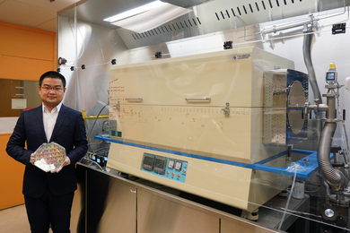
Lightweight and inexpensive, miniaturized mass filters are a key step toward portable mass spectrometers that could identify unknown chemicals in remote settings.

The one-step fabrication process rapidly produces miniature chemical reactors that could be used to detect diseases or analyze substances.

Her demonstration of incorporating lattice strain as a means to enhance performance in scaled silicon devices has informed virtually every high-performance chip manufactured today.

A look at how the MIT professor spent his day after learning he had won the Nobel Prize in Chemistry.

For his work on techniques to generate quantum dots of uniform size and color, Bawendi is honored along with Louis Brus and Alexei Ekimov.
All together, a core group of MIT.nano staffers has more than 400 years of technical experience in nanoscale characterization and fabrication.
A new low-temperature growth and fabrication technology allows the integration of 2D materials directly onto a silicon circuit, which could lead to denser and more powerful chips.

The device would be a key component of a portable mass spectrometer that could help monitor pollutants, perform medical diagnoses in remote areas, or test Martian soil.
A hands-on class teaches undergraduates the fundamentals of quantum mechanics and nanoscale science from inside MIT.nano’s cleanroom.