Skip to content ↓

MIT.nano Family Day invites those at home to come to work

Staff share nano experience — and ice cream — with their families.
Press Inquiries

Press Contact:

Tom Gearty
Phone: 617-253-3951
MIT.nano
Close
A collage of six photos showing groups of people at MIT.nano family day.
Caption:
MIT.nano Family Day brought over 50 family members of MIT.nano staff to MIT for a fun-filled day of nanoscale exploration.
Credits:
Photo collage: Tom Gearty
A group of people wearing white, protective "bunny suits" are seen through a window into a laboratory.
Caption:
After learning how to gown up in a bunny suit, family members took a tour of MIT.nano’s cleanroom.
Credits:
Photo: Tom Gearty
Nicholas Menounos leads a group of adults and children down a hallway filled with pumps and machines.
Caption:
Associate Director for Infrastructure Nicholas Menounos leads family members on a behind-the-scenes tour of some of MIT.nano’s infrastructure spaces.
Credits:
Photo: Tom Gearty
An adult with his arm around a child; both are wearing full-body, protective "bunny suits."
Caption:
Assistant Director of Operations Kristofor Payer shows his son how to gown up in a bunny suit before entering the cleanroom.
Credits:
Photo courtesy of MIT.nano.
A young girl wears a virtual reality headset
Caption:
Charlotte Gearty, daughter of Director of Communications and Initiatives Tom Gearty, visits a virtual world using a mixed-reality headset in the MIT.nano Immersion Lab.
Credits:
Photo: Tom Gearty
Sarah Sterling reaches her arm into a tangle of wires and metal parts inside a large microscope instrument.
Caption:
In one of MIT.nano’s characterization suites, CryoEM Facility Director Sarah Sterling explains the inner workings of a Talos Arctica cryogenic transmission electron microscope.
Credits:
Photo: Tom Gearty
In a cleanroom suffused with amber-colored light, a person in a full bunny suit reaches into a large instrument holding a container of silicon wafers.
Caption:
A smaller group of volunteers joined MIT.nano staff in using the cleanroom processing tools to expose, develop, and etch a Family Day group photo onto a 50-nanometer-thick layer of aluminum on a silicon wafer. Here, one family member loads the PicoTrack under the direction of Research Associate Kurt Broderick.
Credits:
Photo courtesy of MIT.nano.
A circular silicon wafer displaying a group photo of 50 people.
Caption:
The MIT.nano Family Day 2023 wafer is now on display in MIT.nano’s first floor cleanroom window, just outside the West Lobby of the Lisa T. Su Building.
Credits:
Photo courtesy of MIT.nano.
A family of five poses for the camera
Caption:
MIT.nano Director Vladimir Bulović (second from right) poses with his family at MIT.nano Family Day.
Credits:
Photo: Tom Gearty
A line of people standing alongside an ice cream truck called Snowy Joey’s
Caption:
MIT.nano Family Day concluded with an ice cream social and swag grab in MIT.nano’s courtyard.
Credits:
Photo: Tom Gearty

Every day, researchers come to MIT.nano to investigate at the nanoscale, but what’s it like to work there? On Aug. 21, MIT.nano staff invited their family members to come see what it takes to support discovery, education, and innovation in this cutting-edge research facility.

More than 50 people attended — spouses and partners, parents and children, nephews and nieces, in-laws, and others. The event was so much fun that staff and families alike were asking to do it again; by the end of the day calling it the “first annual” MIT.nano Family Day.

After a welcome from Vladimir Bulović, faculty director of MIT.nano and Fariborz Maseeh Professor of Emerging Technologies, technical staff introduced the families to the building and its various facilities. Following a behind-the-scenes tour of some of the infrastructure spaces, they enjoyed lunch in MIT.nano’s East Lobby, then split into groups for hands-on experiences throughout the building.

In MIT.nano’s characterization facility, visitors gained a firsthand look at the powerful microscopes positioned inside the basement imaging suites and learned how to minimize vibrational and electromagnetic interference in order to make videos of atoms. In one suite, the guests viewed individual columns of atoms using an aberration-corrected scanning transmission electron microscope. In another, staff demonstrated how to use micro-computed tomography (microCT) to obtain three-dimensional imagery of the interior of electronic devices, biological samples, and other objects.

The next stop was the MIT.nano Immersion Lab for demonstrations of sensing technology and immersive experiences. Family members put on a mixed-reality headset and were transported — virtually — into the cockpit of an airplane preparing for takeoff. Those not interested in flying stepped inside a virtual art studio complete with balloons on the ceiling and snow falling outside.

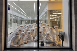
Family members also donned full-body protective clothing called “bunny suits” and headed into MIT.nano’s cleanroom. As they toured the nanofabrication facility, the visitors observed researchers operating equipment and tested a particle counter that illustrated just how much of a wrecking ball dust can be at the nanoscale. A smaller group of volunteers joined MIT.nano staff in using the cleanroom processing tools to expose, develop, and etch a Family Day group photo onto a 50-nanometer-thick layer of aluminum on a silicon wafer, now displayed in MIT.nano’s first floor cleanroom window.

The day concluded with an ice cream social and swag grab in MIT.nano’s courtyard, where staff and their visitors mingled with one another as a new, extended MIT and MIT.nano family.

Related Links

Related Topics

Related Articles

More MIT News