Quantum computers are experimental devices that offer large speedups on some computational problems. One promising approach to building them involves harnessing nanometer-scale atomic defects in diamond materials.
But practical, diamond-based quantum computing devices will require the ability to position those defects at precise locations in complex diamond structures, where the defects can function as qubits, the basic units of information in quantum computing. In today’s of Nature Communications, a team of researchers from MIT, Harvard University, and Sandia National Laboratories reports a new technique for creating targeted defects, which is simpler and more precise than its predecessors.
In experiments, the defects produced by the technique were, on average, within 50 nanometers of their ideal locations.
“The dream scenario in quantum information processing is to make an optical circuit to shuttle photonic qubits and then position a quantum memory wherever you need it,” says Dirk Englund, an associate professor of electrical engineering and computer science who led the MIT team. “We’re almost there with this. These emitters are almost perfect.”
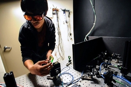
The new paper has 15 co-authors. Seven are from MIT, including Englund and first author Tim Schröder, who was a postdoc in Englund’s lab when the work was done and is now an assistant professor at the University of Copenhagen’s Niels Bohr Institute. Edward Bielejec led the Sandia team, and physics professor Mikhail Lukin led the Harvard team.
Appealing defects
Quantum computers, which are still largely hypothetical, exploit the phenomenon of quantum “superposition,” or the counterintuitive ability of small particles to inhabit contradictory physical states at the same time. An electron, for instance, can be said to be in more than one location simultaneously, or to have both of two opposed magnetic orientations.
Where a bit in a conventional computer can represent zero or one, a “qubit,” or quantum bit, can represent zero, one, or both at the same time. It’s the ability of strings of qubits to, in some sense, simultaneously explore multiple solutions to a problem that promises computational speedups.
Diamond-defect qubits result from the combination of “vacancies,” which are locations in the diamond’s crystal lattice where there should be a carbon atom but there isn’t one, and “dopants,” which are atoms of materials other than carbon that have found their way into the lattice. Together, the dopant and the vacancy create a dopant-vacancy “center,” which has free electrons associated with it. The electrons’ magnetic orientation, or “spin,” which can be in superposition, constitutes the qubit.
A perennial problem in the design of quantum computers is how to read information out of qubits. Diamond defects present a simple solution, because they are natural light emitters. In fact, the light particles emitted by diamond defects can preserve the superposition of the qubits, so they could move quantum information between quantum computing devices.
Silicon switch
The most-studied diamond defect is the nitrogen-vacancy center, which can maintain superposition longer than any other candidate qubit. But it emits light in a relatively broad spectrum of frequencies, which can lead to inaccuracies in the measurements on which quantum computing relies.
In their new paper, the MIT, Harvard, and Sandia researchers instead use silicon-vacancy centers, which emit light in a very narrow band of frequencies. They don’t naturally maintain superposition as well, but theory suggests that cooling them down to temperatures in the millikelvin range — fractions of a degree above absolute zero — could solve that problem. (Nitrogen-vacancy-center qubits require cooling to a relatively balmy 4 kelvins.)
To be readable, however, the signals from light-emitting qubits have to be amplified, and it has to be possible to direct them and recombine them to perform computations. That’s why the ability to precisely locate defects is important: It’s easier to etch optical circuits into a diamond and then insert the defects in the right places than to create defects at random and then try to construct optical circuits around them.
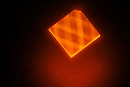
In the process described in the new paper, the MIT and Harvard researchers first planed a synthetic diamond down until it was only 200 nanometers thick. Then they etched optical cavities into the diamond’s surface. These increase the brightness of the light emitted by the defects (while shortening the emission times).
Then they sent the diamond to the Sandia team, who have customized a commercial device called the Nano-Implanter to eject streams of silicon ions. The Sandia researchers fired 20 to 30 silicon ions into each of the optical cavities in the diamond and sent it back to Cambridge.
Mobile vacancies
At this point, only about 2 percent of the cavities had associated silicon-vacancy centers. But the MIT and Harvard researchers have also developed processes for blasting the diamond with beams of electrons to produce more vacancies, and then heating the diamond to about 1,000 degrees Celsius, which causes the vacancies to move around the crystal lattice so they can bond with silicon atoms.
After the researchers had subjected the diamond to these two processes, the yield had increased tenfold, to 20 percent. In principle, repetitions of the processes should increase the yield of silicon vacancy centers still further.
When the researchers analyzed the locations of the silicon-vacancy centers, they found that they were within about 50 nanometers of their optimal positions at the edge of the cavity. That translated to emitted light that was about 85 to 90 percent as bright as it could be, which is still very good.
“It’s an excellent result,” says Jelena Vuckovic, a professor of electrical engineering at Stanford University who studies nanophotonics and quantum optics. “I hope the technique can be improved beyond 50 nanometers, because 50-nanometer misalignment would degrade the strength of the light-matter interaction. But this is an important step in that direction. And 50-nanometer precision is certainly better than not controlling position at all, which is what we are normally doing in these experiments, where we start with randomly positioned emitters and then make resonators.”