
Nanowires — microscopic fibers that can be “grown” in the lab — are a hot research topic today, with a variety of potential applications including light-emitting diodes (LEDs) and sensors. Now, a team of MIT researchers has found a way of precisely controlling the width and composition of these tiny strands as they grow, making it possible to grow complex structures that are optimally designed for particular applications.
The results are described in a new paper authored by MIT assistant professor of materials science and engineering Silvija Gradečak and her team, published in the journal Nano Letters.
Nanowires have been of great interest because structures with such tiny dimensions — typically just a few tens of nanometers, or billionths of a meter, in diameter — can have very different properties than the same materials have in their larger form. That’s in part because at such minuscule scales, quantum confinement effects — based on the behavior of electrons and phonons within the material — begin to play a significant role in the material’s behavior, which can affect how it conducts electricity and heat or interacts with light.
In addition, because nanowires have an especially large amount of surface area in relation to their volume, they are particularly well-suited for use as sensors, Gradečak says.
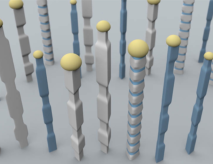
Her team was able to control and vary both the size and composition of individual wires as they grew. Nanowires are grown by using “seed” particles, metal nanoparticles that determine the size and composition of the nanowire. By adjusting the amount of gases used in growing the nanowires, Gradečak and her team were able to control the size and composition of the seed particles and, therefore, the nanowires as they grew. “We’re able to control both of these properties simultaneously,” she says. While the researchers carried out their nanowire-growth experiments with indium nitride and indium gallium nitride, they say the same technique could be applied to a variety of different materials.
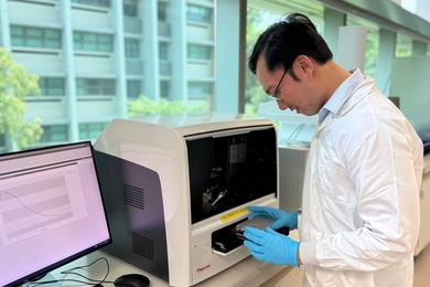
These nanowires are far too small to see with the naked eye, but the team was able to observe them using electron microscopy, making adjustments to the growth process based on what they learned about the growth patterns. Using a process called electron tomography, they were able to reconstruct the three-dimensional shape of individual nanoscale wires. In a related study recently published in the journal Nanoscale, the team also used a unique electron-microscopy technique called cathodoluminescence to observe what wavelengths of light are emitted from different regions of individual nanowires.
Precisely structured nanowires could facilitate a new generation of semiconductor devices, Gradečak says. Such control of nanowire geometry and composition could enable devices with better functionality than conventional thin-film devices made of the same materials, she says.
One likely application of the materials developed by Gradečak and her team is in LED light bulbs, which have far greater durability and are more energy-efficient than other lighting alternatives. The most important colors of light to produce from LEDs are in the blue and ultraviolet range; zinc oxide and gallium nitride nanowires produced by the MIT group can potentially produce these colors very efficiently and at low cost, she says.
While LED light bulbs are available today, they are relatively expensive. “For everyday applications, the high cost is a barrier,” Gradečak says. One big advantage of this new approach is that it could enable the use of much less expensive substrate materials — a major part of the cost of such devices, which today typically use sapphire or silicon carbide substrates. The nanowire devices have the potential to be more efficient as well, she says.
Such nanowires could also find applications in solar-energy collectors for lower-cost solar panels. Being able to control the shape and composition of the wires as they grow could make it possible to produce very efficient collectors: The individual wires form defect-free single crystals, reducing the energy lost due to flaws in the structure of conventional solar cells. And by controlling the exact dimensions of the nanowires, it’s possible to control which wavelengths of light they are “tuned” to, either for producing light in an LED or for collecting light in a solar panel.
Complex structures made of nanowires with varying diameters could also be useful in new thermoelectric devices to capture waste heat and turn it into useful electric power. By varying the composition and diameter of the wires along their length, it’s possible to produce wires that conduct electricity well but heat poorly — a combination that is hard to achieve in most materials, but is key to efficient thermoelectric generating systems.
The nanowires can be produced using tools already in use by the semiconductor industry, so the devices should be relatively easy to gear up for mass production, the team says.
Zhong Lin Wang, the Regents’ Professor and Hightower Chair in Materials Science and Engineering at the Georgia Institute of Technology, says that being able to control the structure and composition of nanowires is “vitally important for controlling their nanoscale properties. The fine-tuning in the growth behavior” of these materials “opens the possibility for fabricating new optoelectronic devices that are likely to have superior performance.”
In addition to Gradečak, the Nano Letters paper was co-authored by MIT graduate student Sam Crawford, Sung Keun Lim PhD ’11 and researcher Georg Haberfehlner of the research and technology organization CEA-Leti in Grenoble, France. The Nanoscale paper was co-authored by MIT graduate student Xiang Zhou, Megan Brewster PhD ’11 and postdoc Ming-Yen Lu. The work was supported by the MIT Center for Excitonics, the U.S. Department of Energy, the MIT-France MISTI program and the National Science Foundation.
The results are described in a new paper authored by MIT assistant professor of materials science and engineering Silvija Gradečak and her team, published in the journal Nano Letters.
Nanowires have been of great interest because structures with such tiny dimensions — typically just a few tens of nanometers, or billionths of a meter, in diameter — can have very different properties than the same materials have in their larger form. That’s in part because at such minuscule scales, quantum confinement effects — based on the behavior of electrons and phonons within the material — begin to play a significant role in the material’s behavior, which can affect how it conducts electricity and heat or interacts with light.
In addition, because nanowires have an especially large amount of surface area in relation to their volume, they are particularly well-suited for use as sensors, Gradečak says.
Her team was able to control and vary both the size and composition of individual wires as they grew. Nanowires are grown by using “seed” particles, metal nanoparticles that determine the size and composition of the nanowire. By adjusting the amount of gases used in growing the nanowires, Gradečak and her team were able to control the size and composition of the seed particles and, therefore, the nanowires as they grew. “We’re able to control both of these properties simultaneously,” she says. While the researchers carried out their nanowire-growth experiments with indium nitride and indium gallium nitride, they say the same technique could be applied to a variety of different materials.
These nanowires are far too small to see with the naked eye, but the team was able to observe them using electron microscopy, making adjustments to the growth process based on what they learned about the growth patterns. Using a process called electron tomography, they were able to reconstruct the three-dimensional shape of individual nanoscale wires. In a related study recently published in the journal Nanoscale, the team also used a unique electron-microscopy technique called cathodoluminescence to observe what wavelengths of light are emitted from different regions of individual nanowires.
Precisely structured nanowires could facilitate a new generation of semiconductor devices, Gradečak says. Such control of nanowire geometry and composition could enable devices with better functionality than conventional thin-film devices made of the same materials, she says.
One likely application of the materials developed by Gradečak and her team is in LED light bulbs, which have far greater durability and are more energy-efficient than other lighting alternatives. The most important colors of light to produce from LEDs are in the blue and ultraviolet range; zinc oxide and gallium nitride nanowires produced by the MIT group can potentially produce these colors very efficiently and at low cost, she says.
While LED light bulbs are available today, they are relatively expensive. “For everyday applications, the high cost is a barrier,” Gradečak says. One big advantage of this new approach is that it could enable the use of much less expensive substrate materials — a major part of the cost of such devices, which today typically use sapphire or silicon carbide substrates. The nanowire devices have the potential to be more efficient as well, she says.
Such nanowires could also find applications in solar-energy collectors for lower-cost solar panels. Being able to control the shape and composition of the wires as they grow could make it possible to produce very efficient collectors: The individual wires form defect-free single crystals, reducing the energy lost due to flaws in the structure of conventional solar cells. And by controlling the exact dimensions of the nanowires, it’s possible to control which wavelengths of light they are “tuned” to, either for producing light in an LED or for collecting light in a solar panel.
Complex structures made of nanowires with varying diameters could also be useful in new thermoelectric devices to capture waste heat and turn it into useful electric power. By varying the composition and diameter of the wires along their length, it’s possible to produce wires that conduct electricity well but heat poorly — a combination that is hard to achieve in most materials, but is key to efficient thermoelectric generating systems.
The nanowires can be produced using tools already in use by the semiconductor industry, so the devices should be relatively easy to gear up for mass production, the team says.
Zhong Lin Wang, the Regents’ Professor and Hightower Chair in Materials Science and Engineering at the Georgia Institute of Technology, says that being able to control the structure and composition of nanowires is “vitally important for controlling their nanoscale properties. The fine-tuning in the growth behavior” of these materials “opens the possibility for fabricating new optoelectronic devices that are likely to have superior performance.”
In addition to Gradečak, the Nano Letters paper was co-authored by MIT graduate student Sam Crawford, Sung Keun Lim PhD ’11 and researcher Georg Haberfehlner of the research and technology organization CEA-Leti in Grenoble, France. The Nanoscale paper was co-authored by MIT graduate student Xiang Zhou, Megan Brewster PhD ’11 and postdoc Ming-Yen Lu. The work was supported by the MIT Center for Excitonics, the U.S. Department of Energy, the MIT-France MISTI program and the National Science Foundation.