Microelectromechanical devices — tiny machines with moving parts — are everywhere these days: they monitor air pressure in car tires, register the gestures of video game players, and reflect light onto screens in movie theaters. But they’re manufactured the same way computer chips are, in facilities that can cost billions of dollars, and their rigidity makes them hard to wrap around curved surfaces.
MIT researchers have discovered a way to make microelectromechanical devices, or MEMS, by stamping them onto a plastic film. That should significantly reduce their cost, but it also opens up the possibility of large sheets of sensors that could, say, cover the wings of an airplane to gauge their structural integrity. The printed MEMS are also flexible, so they could be used to make sensors with irregular shapes. And since the stamping process dispenses with the harsh chemicals and high temperatures ordinarily required for the fabrication of MEMS, it could allow MEMS to incorporate a wider range of materials.
Conventional MEMS are built through a process called photolithography, in which different layers of material are chemically deposited on a substrate — usually a wafer of some semiconducting material — and etched away to form functional patterns. Since a wafer is at most 12 inches across, arranging today’s MEMS into large arrays requires cutting them out and bonding them to some other surface.
Instead of using a wafer, the MIT researchers begin with a grooved sheet of a rubbery plastic, which is coated with the electrically conductive material indium tin oxide. The researchers use what they call a “transfer pad” to press a thin film of metal against the grooved plastic. Between the metal film and the pad is a layer of organic molecules that weaken the metal’s adhesion to the pad. If the researchers pull the pad away fast enough, the metal remains stuck to the plastic.
“It’s kind of similar to if you have Scotch tape on a piece of paper,” says Corinne Packard, a postdoc in the Research Lab of Electronics at MIT who led the work, along with professors of electrical engineering Vladimir Bulović and Martin Schmidt. “If you peel it off slowly, you can delaminate the tape very easily. But if you peel fast, you’ll rip the paper.”
Once the transfer pad has been ripped away, the metal film is left spanning the grooves in the plastic like a bridge across a series of ravines. Applying a voltage between the indium-tin-oxide coating and the film can cause it to bend downward, into the groove in the plastic: the film becomes an “actuator” — the moving part in a MEMS. Varying the voltage would cause the film to vibrate, like the diaphragm of a loudspeaker; selectively bending different parts of the film would cause them to reflect light in different ways; and dramatically bending the film could turn a smooth surface into a rough one. Similarly, if pressure is applied to the metal film, it will generate an electric signal that the researchers can detect. The film is so thin that it should be able to register the pressure of sound waves.
Serendipity
The discovery of the manufacturing technique, which the MIT team describes in a forthcoming issue of the journal Advanced Materials, was a happy accident. The researchers were actually trying to use a printing technique to build an electrical circuit. They had created a plastic stamp with a pattern molded into it and were trying to transfer that pattern to a thin sliver film. They had expected that the plastic would pull away the silver it made contact with, leaving behind an electrode that could control an organic light-emitting diode.
Instead, however, the stamp kept pulling away the entire silver film. “The first couple times we did this, we were like, ‘Ah! Bummer, man,’” says Bulović. “And then a light bulb went off, and we said, ‘Well, but we just made the world’s first printed MEM.’” The stamp was intended as a means of creating an electronic device; instead, it ended up serving as the basis for a device itself. The researchers’ ensuing work was on the ideal architecture for the device and on ways to minimize the metal film’s adhesion to the transfer pad and maximize its adhesion to the grooved plastic.
Because the researchers hadn’t set out to make MEMS, and because, to their knowledge, their films constitute the first stamped MEMS devices, they’re still trying to determine the ideal application of the technology. Sheets of sensors to gauge the structural integrity of aircraft and bridges are one possibility; but the MEMS could also change the physical texture of the surfaces they’re applied to, altering the airflow over a wing, or modifying the reflective properties of a building’s walls or windows. A sheet of thousands of tiny microphones could determine, from the difference in the time at which sound waves arrive at different points, where a particular sound originated. Such a system could filter out extraneous sounds in a noisy room, or even perform echolocation, the way bats do. The same type of sheet could constitute a paper-thin loudspeaker; the vibrations of different MEMS might even be designed to interfere with each other, so that transmitted sounds would be perfectly audible at some location but inaudible a few feet away. The technology could also lead to large digital displays that could be rolled up when not in use.
John Rogers, a researcher at the University of Illinois at Urbana-Champaign who has pioneered techniques for printable electrical circuits, is particularly intrigued by the idea that printable MEMS could incorporate materials that are incompatible with existing MEMS manufacturing processes. “The ability to do heterogeneous integration of different material types into micromachines is a neat capability that would be enabled by this form of manufacturing,” Rogers says. “It opens up new design opportunities because it relaxes constraints on choices of materials.” And in general, Rogers says, the idea of printing MEMS is “cool.” “What they’ve done in this paper is demonstrated, for the first time, to my knowledge, this kind of concept.”
Microelectromechanical devices gave us the Wii and the digital movie projector. MIT researchers have found a new way to make them.
Publication Date:
Caption:
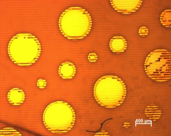
To test a new technique for creating micromachines, MIT researchers deposited films of gold on a sheet of plastic; grooves in the plastic are visible as a series of horizontal lines.
Credits:
Image: Corinne Packard and Apoorva Murarka
Caption:
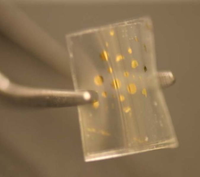
Unlike existing micromachines, the researchers' gold films are flexible, so they could be used to coat irregular surfaces.
Credits:
Photo: Corinne Packard


