An MIT faculty member has come up with a quick and easy test which, with the pulse of a laser, can analyze the thin films used in microelectronics components. The same optical method may one day be used to provide an early-warning signal for eye disease or to "optically switch" materials from one phase to another.
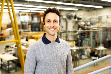
All this is part of a program developed by Professor of Chemistry Keith A. Nelson, a member of the Materials Processing Center and the Center for Materials Science and Engineering. He and his research group study how materials respond when they are irradiated by pulsed laser light.
Applications for this work range from adding to basic knowledge about complex materials to the practical test for thin films that may save the microelectronics industry millions of dollars each year in testing costs.
Another far-off goal is the ability to "optically control" the structure and behavior of materials, with intriguing prospects including ultrafast optical signal processing and optical fabrication of unique material structures.
"Much of the 'art' in our efforts comes through understanding how light, especially in the form of short pulses, interacts with matter and how the interactions can be exploited to characterize or control materials," Professor Nelson said.
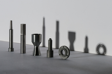
In microelectronics manufacturing, a silicon base is coated with one thin layer after another. Copper, tungsten and other metal layers have precisely specified thicknesses that range from 100 angstroms, or about how much a fingernail grows in one second, to 10,000 angstroms, or one-thousandth of a millimeter. Variation in the thickness of the metal layers is a major cause of device failure and low microelectronics manufacturing yields.
To make sure that each film layer is the right thickness and is properly adhered to the layer below it, manufacturers have had to perform painstaking tests with expensive equipment. These tests destroy the sample, at huge cost to the industry. Professor Nelson's nondestructive, noncontact optical test, which uses a laser device that fits into a briefcase, can measure film thickness to within about one layer of atoms (1-3 angstroms) in one second, and at the same time check for proper adhesion.
The device, which incorporates a mini-laser half a thumb's-length that was developed by Lincoln Laboratory, has been developed commercially in the past two years by a start-up company formed by Professor Nelson and two of his former graduate students, John A. Rogers (PhD 1995) and Matt Banet (PhD 1993). Because of the device's promise and early industry acceptance, the company was wholly acquired last summer by Philips Analytical N.V. (part of the same Philips that makes CDs and CD players). The instrument is now in use at locations around the world.
The instrument uses short laser pulses to generate ultrasonic waves&emdash;sound vibrations beyond the range of human hearing&emdash;in the thin film. Light from a second laser is used to monitor the acoustic waves and determine their velocity, which depends on the thickness and adhesion of the film.
"The device doesn't require difficult adjustments, and you don't need a laser jock or a PhD scientist to do the analysis or get the numbers out," Professor Nelson said. In fact, the optical part of the instrument is entirely enclosed and out of view of the user, who simply pushes buttons to start the measurement.
By comparing the signal from a sample coming off the assembly line to that expected from a perfect component, the user can figure out if the sample is just right or if it was flawed in the manufacturing process. In addition to microelectronics materials, thin films that could be tested with Professor Nelson's measurement method include optical elements like filters and mirrors, liquid-crystal displays and ultrahard coatings.
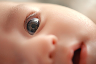
Many kinds of polymer films, including biopolymers like the cornea of the eye, can also be examined. The main requirement is that the sample be smooth and shiny enough to reflect light without too much scatter.
In related work led by current graduate students Timothy Crimmins and Richard Koehl, Professor Nelson has experimented with ultrashort pulses of light to optically control the structure of crystalline solids by moving atoms from their initial positions along selected microscopic pathways toward the positions they would occupy in a new crystalline structure.
SWITCHING STRUCTURES
Although this objective is still far off, the technique may one day make it possible to "optically switch" a material from one structure to another, even without any absorption of the light. Like an ice crystal, which can assume nine different forms (popularized in Kurt Vonnegut's sci-fi story in which a mad scientist tries to freeze the Earth by turning the oceans into "ice nine"), other crystals may be altered by rearranging their structure from that of one phase to another.
This method may make it possible to "optically control" a material by changing the configuration of its molecular infrastructure, and even to create new states of existing materials by forcing their atoms into configurations they wouldn't normally assume, Professor Nelson said.
His research group recently succeeded in "shaping" a pulse of light lasting less than one-quadrillionth of a second into a timed sequence of pulses that can launch vibrational waves in a crystal with larger and larger amplitude. The pulses of light "push" at the crystal lattice framework much like a person pushing a child on a swing, causing ever-larger excursions from the original position. If sufficiently large motions can be induced, the material could enter a new crystalline phase.
Very recently, Professor Nelson's group has been able to shape a single light pulse into not just one timed pulse sequence, but many pulse sequences that can reach different regions of a sample. In this manner, the researchers can continue to manipulate and amplify thevibrational wave as it travels through the crystal at light-like speed. This advance offers prospects for optical control over ultrafast signals and brings the dream of optical control over material structure one step closer to realization.
Professor Nelson's work is supported by the National Science Foundation, the Office of Naval Research and the Army Research Office.
A version of this article appeared in the March 3, 1999 issue of MIT Tech Talk (Volume 43, Number 21).

